参数资料
| 型号: | X9110TV14ZT1 |
| 厂商: | Intersil |
| 文件页数: | 1/18页 |
| 文件大小: | 0K |
| 描述: | IC XDCP 1024-TAP 100K 14-TSSOP |
| 标准包装: | 2,500 |
| 系列: | XDCP™ |
| 接片: | 1024 |
| 电阻(欧姆): | 100k |
| 电路数: | 1 |
| 温度系数: | 标准值 ±300 ppm/°C |
| 存储器类型: | 非易失 |
| 接口: | 4 线 SPI(芯片选择,设备位址) |
| 电源电压: | 4.5 V ~ 5.5 V |
| 工作温度: | 0°C ~ 70°C |
| 安装类型: | 表面贴装 |
| 封装/外壳: | 14-TSSOP(0.173",4.40mm 宽) |
| 供应商设备封装: | 14-TSSOP |
| 包装: | 带卷 (TR) |
1
FN8158.3
CAUTION: These devices are sensitive to electrostatic discharge; follow proper IC Handling Procedures.
1-888-INTERSIL or 1-888-468-3774
| Intersil (and design) is a registered trademark of Intersil Americas Inc.
XDCP is a trademark of Intersil Americas INC. Copyright Intersil Americas Inc. 2005, 2008. All Rights Reserved
All other trademarks mentioned are the property of their respective owners.
X9110
Dual Supply/Low Power/1024-Tap/SPI Bus
Single Digitally-Controlled (XDCP)
Potentiometer
The X9110 integrates a single digitally controlled
potentiometer (XDCP) on a monolithic CMOS integrated
circuit.
The digital controlled potentiometer is implemented using
1023 resistive elements in a series array. Between each
element are tap points connected to the wiper terminal
through switches. The position of the wiper on the array is
controlled by the user through the SPI bus interface. The
potentiometer has associated with it a volatile Wiper Counter
Register (WCR) and four non-volatile Data Registers that
can be directly written to and read by the user. The contents
of the WCR controls the position of the wiper on the resistor
array though the switches. Power-up recalls the contents of
the default data register (DR0) to the WCR.
The XDCP can be used as a three-terminal potentiometer or
as a two terminal variable resistor in a wide variety of
applications including control, parameter adjustments, and
signal processing.
Features
1024 Resistor Taps – 10-Bit Resolution
SPI Serial Interface for write, read, and transfer operations
of the potentiometer
Wiper Resistance, 40
Ω Typical @ 5V
Four Non-Volatile Data Registers
Non-Volatile Storage of Multiple Wiper Positions
Power-on Recall. Loads Saved Wiper Position on Power-up
Standby Current < 3A Max
System VCC: 2.7V to 5.5V Operation
Analog V+/V-: -5V to +5V
100k
Ω End to End Resistance
100 yr. Data Retention
Endurance: 100, 000 Data Changes Per Bit Per Register
14 Ld TSSOP
Dual Supply Version of the X9111
Low Power CMOS
Pb-Free Available (RoHS Compliant)
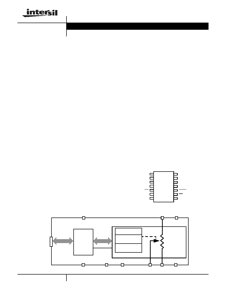
Pinout
X9110
14 LD TSSOP
TOP VIEW
Functional Diagram
VCC
RL
VSS
1
2
3
4
5
6
7
8
14
13
12
11
10
9
A0
RW
SCK
CS
RH
S0
V+
SI
HOLD
WP
V-
RH
RL
BUS
RW
INTERFACE &
CONTROL
POT
VCC
VSS
SPI
BUS
ADDRESS
DATA
STATUS
WRITE
READ
WIPER
1024-TAPS
TRANSFER
NC
100k
Ω
POWER-ON RECALL
WIPER COUNTER
REGISTER (WCR)
DATA REGISTERS
(DR0-DR3)
CONTROL
INTERFACE
V+
V-
Data Sheet
February 13, 2008
相关PDF资料 |
PDF描述 |
|---|---|
| MS3452L28-21P | CONN RCPT 37POS BOX MNT W/PINS |
| X9420YS16Z-2.7 | IC DGTL POT 2.5K 1CH 16SOIC |
| VI-JV2-MZ-S | CONVERTER MOD DC/DC 15V 25W |
| M83723/82G08039 | CONN RCPT 3POS WALL MT W/SCKT |
| VI-J4H-MZ-S | CONVERTER MOD DC/DC 52V 25W |
相关代理商/技术参数 |
参数描述 |
|---|---|
| X9111 | 制造商:INTERSIL 制造商全称:Intersil Corporation 功能描述:Single Supply/Low Power/1024-Tap/SPI Bus |
| X9111_06 | 制造商:INTERSIL 制造商全称:Intersil Corporation 功能描述:Single Digitally-Controlled (XDCP⑩) Potentiometer |
| X9111TB15 | 制造商:XICOR 制造商全称:Xicor Inc. 功能描述:Single Digitally-Controlled Potentiometer |
| X9111TB15-2.7 | 制造商:XICOR 制造商全称:Xicor Inc. 功能描述:Single Digitally-Controlled Potentiometer |
| X9111TB15I | 制造商:XICOR 制造商全称:Xicor Inc. 功能描述:Single Digitally-Controlled Potentiometer |
发布紧急采购,3分钟左右您将得到回复。