参数资料
| 型号: | XC2S100-5FG256I |
| 厂商: | Xilinx Inc |
| 文件页数: | 18/99页 |
| 文件大小: | 0K |
| 描述: | IC FPGA 2.5V I-TEMP 256-FBGA |
| 标准包装: | 90 |
| 系列: | Spartan®-II |
| LAB/CLB数: | 600 |
| 逻辑元件/单元数: | 2700 |
| RAM 位总计: | 40960 |
| 输入/输出数: | 176 |
| 门数: | 100000 |
| 电源电压: | 2.375 V ~ 2.625 V |
| 安装类型: | 表面贴装 |
| 工作温度: | -40°C ~ 100°C |
| 封装/外壳: | 256-BGA |
| 供应商设备封装: | 256-FBGA(17x17) |
第1页第2页第3页第4页第5页第6页第7页第8页第9页第10页第11页第12页第13页第14页第15页第16页第17页当前第18页第19页第20页第21页第22页第23页第24页第25页第26页第27页第28页第29页第30页第31页第32页第33页第34页第35页第36页第37页第38页第39页第40页第41页第42页第43页第44页第45页第46页第47页第48页第49页第50页第51页第52页第53页第54页第55页第56页第57页第58页第59页第60页第61页第62页第63页第64页第65页第66页第67页第68页第69页第70页第71页第72页第73页第74页第75页第76页第77页第78页第79页第80页第81页第82页第83页第84页第85页第86页第87页第88页第89页第90页第91页第92页第93页第94页第95页第96页第97页第98页第99页
Spartan-II FPGA Family: Functional Description
DS001-2 (v2.8) June 13, 2008
Module 2 of 4
Product Specification
25
R
If CCLK is slower than FCCNH, the FPGA will never assert
BUSY. In this case, the above handshake is unnecessary,
and data can simply be entered into the FPGA every CCLK
cycle.
A configuration packet does not have to be written in one
continuous stretch, rather it can be split into many write
sequences. Each sequence would involve assertion of CS.
In applications where multiple clock cycles may be required
to access the configuration data before each byte can be
loaded into the Slave Parallel interface, a new byte of data
may not be ready for each consecutive CCLK edge. In such
a case the CS signal may be de-asserted until the next byte
is valid on D0-D7. While CS is High, the Slave Parallel
interface does not expect any data and ignores all CCLK
transitions. However, to avoid aborting configuration,
WRITE must continue to be asserted while CS is asserted.
Abort
To abort configuration during a write sequence, de-assert
WRITE while holding CS Low. The abort operation is
initiated at the rising edge of CCLK, as shown in Figure 21,
page 26. The device will remain BUSY until the aborted
operation is complete. After aborting configuration, data is
assumed to be unaligned to word boundaries and the FPGA
requires a new synchronization word prior to accepting any
new packets.
Boundary-Scan Mode
In the boundary-scan mode, no nondedicated pins are
required, configuration being done entirely through the
IEEE 1149.1 Test Access Port.
Configuration through the TAP uses the special CFG_IN
instruction. This instruction allows data input on TDI to be
converted into data packets for the internal configuration
bus.
The following steps are required to configure the FPGA
through the boundary-scan port.
1.
Load the CFG_IN instruction into the boundary-scan
instruction register (IR)
2.
Enter the Shift-DR (SDR) state
3.
Shift a standard configuration bitstream into TDI
4.
Return to Run-Test-Idle (RTI)
5.
Load the JSTART instruction into IR
6.
Enter the SDR state
7.
Clock TCK through the sequence (the length is
programmable)
8.
Return to RTI
Configuration and readback via the TAP is always available.
The boundary-scan mode simply locks out the other modes.
The boundary-scan mode is selected by a <10x> on the
mode pins (M0, M1, M2).
Readback
The configuration data stored in the Spartan-II FPGA
configuration memory can be readback for verification.
Along with the configuration data it is possible to readback
the contents of all flip-flops/latches, LUT RAMs, and block
RAMs. This capability is used for real-time debugging.
For more detailed information see XAPP176, Spartan-II
FPGA Family Configuration and Readback.
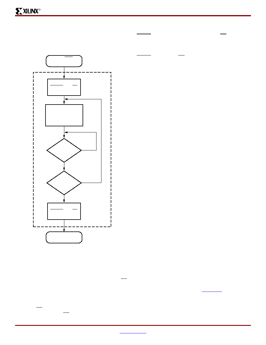
Figure 19: Loading Configuration Data for the Slave
Parallel Mode
Yes
No
FPGA
Driving BUSY
High?
After INIT
Goes High
Load One
Configuration
Byte on Next
CCLK Rising Edge
To CRC Check
DS001_19_032300
No
End of
Configuration
Data File?
Yes
User Drives
WRITE and CS
Low
User Drives
WRITE and CS
High
相关PDF资料 |
PDF描述 |
|---|---|
| 93LC76B-E/SN | IC EEPROM 8KBIT 2MHZ 8SOIC |
| XC6SLX16-3CPG196I | IC FPGA SPARTAN 6 14K 196CPGBGA |
| 25LC020AT-E/OT | IC EEPROM 2KBIT 10MHZ SOT23-6 |
| 24LC16BT-E/MC | IC EEPROM 16KBIT 400KHZ 8DFN |
| 24FC64T-I/ST | IC EEPROM 64KBIT 1MHZ 8TSSOP |
相关代理商/技术参数 |
参数描述 |
|---|---|
| XC2S1005FG456C | 制造商:Xilinx 功能描述: |
| XC2S100-5FG456C | 功能描述:IC FPGA 2.5V 600 CLB'S 456-FBGA RoHS:否 类别:集成电路 (IC) >> 嵌入式 - FPGA(现场可编程门阵列) 系列:Spartan®-II 标准包装:24 系列:ECP2 LAB/CLB数:1500 逻辑元件/单元数:12000 RAM 位总计:226304 输入/输出数:131 门数:- 电源电压:1.14 V ~ 1.26 V 安装类型:表面贴装 工作温度:0°C ~ 85°C 封装/外壳:208-BFQFP 供应商设备封装:208-PQFP(28x28) |
| XC2S100-5FG456I | 功能描述:IC FPGA 2.5V I-TEMP 456-FBGA RoHS:否 类别:集成电路 (IC) >> 嵌入式 - FPGA(现场可编程门阵列) 系列:Spartan®-II 产品变化通告:XC4000(E,L) Discontinuation 01/April/2002 标准包装:24 系列:XC4000E/X LAB/CLB数:100 逻辑元件/单元数:238 RAM 位总计:3200 输入/输出数:80 门数:3000 电源电压:4.5 V ~ 5.5 V 安装类型:表面贴装 工作温度:-40°C ~ 100°C 封装/外壳:120-BCBGA 供应商设备封装:120-CPGA(34.55x34.55) |
| XC2S100-5FGG256C | 功能描述:IC SPARTAN-II FPGA 100K 256-FBGA RoHS:是 类别:集成电路 (IC) >> 嵌入式 - FPGA(现场可编程门阵列) 系列:Spartan®-II 标准包装:40 系列:Spartan® 6 LX LAB/CLB数:3411 逻辑元件/单元数:43661 RAM 位总计:2138112 输入/输出数:358 门数:- 电源电压:1.14 V ~ 1.26 V 安装类型:表面贴装 工作温度:-40°C ~ 100°C 封装/外壳:676-BGA 供应商设备封装:676-FBGA(27x27) |
| XC2S100-5FGG256I | 功能描述:IC SPARTAN-II FPGA 100K 256-FBGA RoHS:是 类别:集成电路 (IC) >> 嵌入式 - FPGA(现场可编程门阵列) 系列:Spartan®-II 标准包装:40 系列:Spartan® 6 LX LAB/CLB数:3411 逻辑元件/单元数:43661 RAM 位总计:2138112 输入/输出数:358 门数:- 电源电压:1.14 V ~ 1.26 V 安装类型:表面贴装 工作温度:-40°C ~ 100°C 封装/外壳:676-BGA 供应商设备封装:676-FBGA(27x27) |
发布紧急采购,3分钟左右您将得到回复。