- 您现在的位置:买卖IC网 > PDF目录300144 > XC3020A7PC68I (Xilinx, Inc.) IC-SMD-FPGA PDF资料下载
参数资料
| 型号: | XC3020A7PC68I |
| 厂商: | Xilinx, Inc. |
| 英文描述: | IC-SMD-FPGA |
| 中文描述: | 集成电路贴片的FPGA |
| 文件页数: | 28/76页 |
| 文件大小: | 731K |
| 代理商: | XC3020A7PC68I |
第1页第2页第3页第4页第5页第6页第7页第8页第9页第10页第11页第12页第13页第14页第15页第16页第17页第18页第19页第20页第21页第22页第23页第24页第25页第26页第27页当前第28页第29页第30页第31页第32页第33页第34页第35页第36页第37页第38页第39页第40页第41页第42页第43页第44页第45页第46页第47页第48页第49页第50页第51页第52页第53页第54页第55页第56页第57页第58页第59页第60页第61页第62页第63页第64页第65页第66页第67页第68页第69页第70页第71页第72页第73页第74页第75页第76页
R
XC3000 Series Field Programmable Gate Arrays
7-36
November 9, 1998 (Version 3.1)
Power
Power Distribution
Power for the FPGA is distributed through a grid to achieve
high noise immunity and isolation between logic and I/O.
Inside the FPGA, a dedicated VCC and ground ring sur-
rounding the logic array provides power to the I/O drivers.
An independent matrix of VCC and groundlines supplies the
interior logic of the device. This power distribution grid pro-
vides a stable supply and ground for all internal logic, pro-
viding the external package power pins are all connected
and appropriately decoupled. Typically a 0.1-
F capacitor
connected near the VCC and ground pins will provide ade-
quate decoupling.
Output buffers capable of driving the specified 4- or 8-mA
loads under worst-case conditions may be capable of driv-
ing as much as 25 to 30 times that current in a best case.
Noise can be reduced by minimizing external load capaci-
tance and reducing simultaneous output transitions in the
same direction. It may also be beneficial to locate heavily
loaded output buffers near the ground pads. The I/O Block
output buffers have a slew-limited mode which should be
used where output rise and fall times are not speed critical.
Slew-limited outputs maintain their dc drive capability, but
generate less external reflections and internal noise.
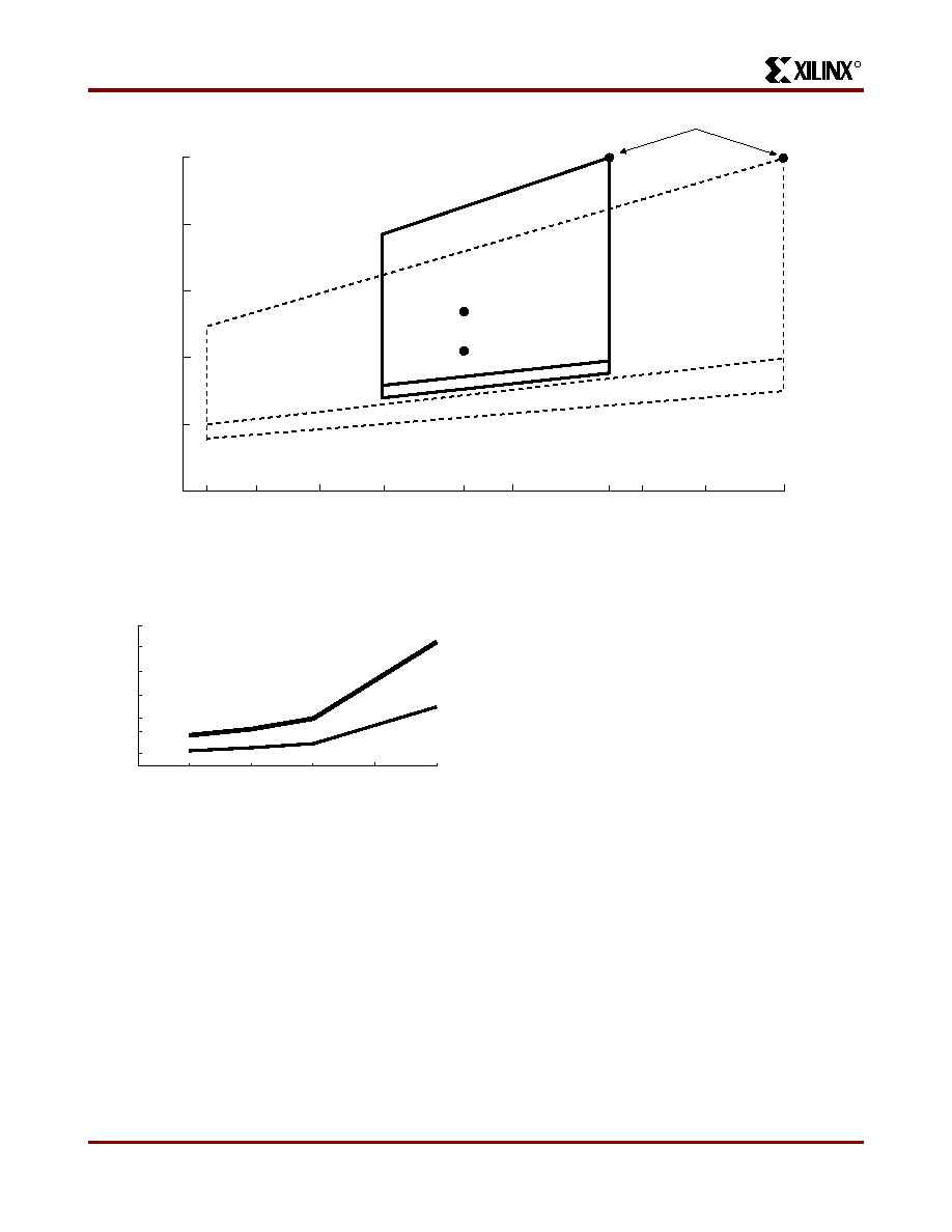
1.00
0.80
0.60
0.40
0.20
SPECIFIED WORST-CASE VALUES
MAX
CO
MMERCIAL
(4.75
V)
MAX
MILITARY
(4.5
V)
– 55
MIN MILITARY
(5.5 V)
MIN COMMERCIAL
(4.75 V)
MIN COMMERCIAL
(5.25 V)
TYPICAL COMMERCIAL
(+ 5.0 V, 25
°C)
TYPICAL MILITARY
TEMPERATURE (
°C)
– 40
– 20
0
25
40
70
80
100
125
NORMALIZED
DELAY
X6094
MIN MILITARY
(4.5 V)
Figure 32: Relative Delay as a Function of Temperature, Supply Voltage and Processing Variations
System
Clock
(MHz)
250
200
150
100
50
3 CLBs
(3-12)
4 CLBs
(4-16)
2 CLBs
(2-8)
1 CLB
(1-4)
XC3100A-3
XC3000A--6
CLB Levels:
Gate Levels:
300
Toggle
Rate
0
X7065
Figure 33: Clock Rate as a Function of Logic
Complexity (Number of Combinational Levels between
Flip-Flops)
相关PDF资料 |
PDF描述 |
|---|---|
| XC3064A-6PQ160C | Field Programmable Gate Array (FPGA) |
| XC3064A-7PQ160I | Field Programmable Gate Array (FPGA) |
| XC4000XLASERIES | Field Programmable Gate Arrays |
| XC4013E-1CB240M | Programmable Gate Arrays |
| XC4013E-1HG240C | Programmable Gate Arrays |
相关代理商/技术参数 |
参数描述 |
|---|---|
| XC3020A-7PC68I | 制造商:XILINX 制造商全称:XILINX 功能描述:Field Programmable Gate Arrays (XC3000A/L, XC3100A/L) |
| XC3020A-7PC84C | 功能描述:IC LOGIC CL ARRAY 2000GAT 84PLCC RoHS:否 类别:集成电路 (IC) >> 嵌入式 - FPGA(现场可编程门阵列) 系列:XC3000A/L 产品变化通告:XC4000(E,L) Discontinuation 01/April/2002 标准包装:24 系列:XC4000E/X LAB/CLB数:100 逻辑元件/单元数:238 RAM 位总计:3200 输入/输出数:80 门数:3000 电源电压:4.5 V ~ 5.5 V 安装类型:表面贴装 工作温度:-40°C ~ 100°C 封装/外壳:120-BCBGA 供应商设备封装:120-CPGA(34.55x34.55) |
| XC3020A-7PC84C0100 | 制造商:Xilinx 功能描述: |
| XC3020A-7PC84I | 制造商:Xilinx 功能描述: |
| XC3020A-7PCG68C | 制造商:Xilinx 功能描述: |
发布紧急采购,3分钟左右您将得到回复。