- 您现在的位置:买卖IC网 > PDF目录300144 > XC3020A7PC68I (Xilinx, Inc.) IC-SMD-FPGA PDF资料下载
参数资料
| 型号: | XC3020A7PC68I |
| 厂商: | Xilinx, Inc. |
| 英文描述: | IC-SMD-FPGA |
| 中文描述: | 集成电路贴片的FPGA |
| 文件页数: | 8/76页 |
| 文件大小: | 731K |
| 代理商: | XC3020A7PC68I |
第1页第2页第3页第4页第5页第6页第7页当前第8页第9页第10页第11页第12页第13页第14页第15页第16页第17页第18页第19页第20页第21页第22页第23页第24页第25页第26页第27页第28页第29页第30页第31页第32页第33页第34页第35页第36页第37页第38页第39页第40页第41页第42页第43页第44页第45页第46页第47页第48页第49页第50页第51页第52页第53页第54页第55页第56页第57页第58页第59页第60页第61页第62页第63页第64页第65页第66页第67页第68页第69页第70页第71页第72页第73页第74页第75页第76页
R
XC3000 Series Field Programmable Gate Arrays
7-18
November 9, 1998 (Version 3.1)
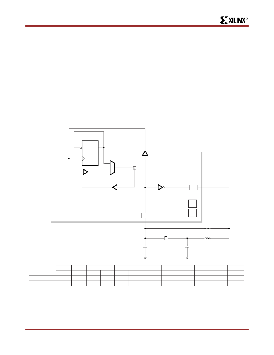
Crystal Oscillator
Figure 18 also shows the location of an internal high speed
inverting amplifier that may be used to implement an
on-chip crystal oscillator. It is associated with the auxiliary
buffer in the lower right corner of the die. When the oscilla-
tor is configured and connected as a signal source, two
special user IOBs are also configured to connect the oscil-
lator amplifier with external crystal oscillator components
as shown in Figure 19. A divide by two option is available to
assure symmetry. The oscillator circuit becomes active
early in the configuration process to allow the oscillator to
stabilize. Actual internal connection is delayed until com-
pletion of configuration. In Figure 19 the feedback resistor
R1, between the output and input, biases the amplifier at
threshold. The inversion of the amplifier, together with the
R-C networks and an AT-cut series resonant crystal, pro-
duce the 360-degree phase shift of the Pierce oscillator. A
series resistor R2 may be included to add to the amplifier
output impedance when needed for phase-shift control,
crystal resistance matching, or to limit the amplifier input
swing to control clipping at large amplitudes. Excess feed-
back voltage may be corrected by the ratio of C2/C1. The
amplifier is designed to be used from 1 MHz to about
one-half the specified CLB toggle frequency. Use at fre-
quencies below 1 MHz may require individual characteriza-
tion with respect to a series resistance. Crystal oscillators
above 20 MHz generally require a crystal which operates in
a third overtone mode, where the fundamental frequency
must be suppressed by an inductor across C2, turning this
parallel resonant circuit to double the fundamental crystal
frequency, i.e., 2/3 of the desired third harmonic frequency
network. When the oscillator inverter is not used, these
IOBs and their package pins are available for general user
I/O.
Alternate
Clock Buffer
XTAL1
XTAL2
(IN)
R1
R2
Y1
C1
C2
Internal
External
R1
R2
C1, C2
Y1
Suggested Component Values
0.5 – 1 M
0 – 1 k
(may be required for low frequency, phase
shift and/or compensation level for crystal Q)
10 – 40 pF
1 – 20 MHz AT-cut parallel resonant
X7064
68 PIN
PLCC
47
43
84 PIN
PLCC
57
53
PGA
J11
L11
132 PIN
PGA
P13
M13
160 PIN
PQFP
82
76
XTAL 1 (OUT)
XTAL 2 (IN)
100 PIN
CQFP
67
61
PQFP
82
76
164 PIN
CQFP
105
99
44 PIN
PLCC
30
26
175 PIN
PGA
T14
P15
208 PIN
PQFP
110
100
176 PIN
TQFP
91
85
D
Q
Figure 19: Crystal Oscillator Inverter. When activated, and by selecting an output network for its buffer, the crystal
oscillator inverter uses two unconfigured package pins and external components to implement an oscillator. An optional
divide-by-two mode is available to assure symmetry.
相关PDF资料 |
PDF描述 |
|---|---|
| XC3064A-6PQ160C | Field Programmable Gate Array (FPGA) |
| XC3064A-7PQ160I | Field Programmable Gate Array (FPGA) |
| XC4000XLASERIES | Field Programmable Gate Arrays |
| XC4013E-1CB240M | Programmable Gate Arrays |
| XC4013E-1HG240C | Programmable Gate Arrays |
相关代理商/技术参数 |
参数描述 |
|---|---|
| XC3020A-7PC68I | 制造商:XILINX 制造商全称:XILINX 功能描述:Field Programmable Gate Arrays (XC3000A/L, XC3100A/L) |
| XC3020A-7PC84C | 功能描述:IC LOGIC CL ARRAY 2000GAT 84PLCC RoHS:否 类别:集成电路 (IC) >> 嵌入式 - FPGA(现场可编程门阵列) 系列:XC3000A/L 产品变化通告:XC4000(E,L) Discontinuation 01/April/2002 标准包装:24 系列:XC4000E/X LAB/CLB数:100 逻辑元件/单元数:238 RAM 位总计:3200 输入/输出数:80 门数:3000 电源电压:4.5 V ~ 5.5 V 安装类型:表面贴装 工作温度:-40°C ~ 100°C 封装/外壳:120-BCBGA 供应商设备封装:120-CPGA(34.55x34.55) |
| XC3020A-7PC84C0100 | 制造商:Xilinx 功能描述: |
| XC3020A-7PC84I | 制造商:Xilinx 功能描述: |
| XC3020A-7PCG68C | 制造商:Xilinx 功能描述: |
发布紧急采购,3分钟左右您将得到回复。