参数资料
| 型号: | XC3S1000-4FGG676I |
| 厂商: | Xilinx Inc |
| 文件页数: | 202/272页 |
| 文件大小: | 0K |
| 描述: | SPARTAN-3A FPGA 1M STD 676-FBGA |
| 产品培训模块: | Extended Spartan 3A FPGA Family |
| 标准包装: | 40 |
| 系列: | Spartan®-3 |
| LAB/CLB数: | 1920 |
| 逻辑元件/单元数: | 17280 |
| RAM 位总计: | 442368 |
| 输入/输出数: | 391 |
| 门数: | 1000000 |
| 电源电压: | 1.14 V ~ 1.26 V |
| 安装类型: | 表面贴装 |
| 工作温度: | -40°C ~ 100°C |
| 封装/外壳: | 676-BGA |
| 供应商设备封装: | 676-FBGA(27x27) |
| 配用: | 122-1502-ND - KIT STARTER SPARTAN-3 PCI-E |
第1页第2页第3页第4页第5页第6页第7页第8页第9页第10页第11页第12页第13页第14页第15页第16页第17页第18页第19页第20页第21页第22页第23页第24页第25页第26页第27页第28页第29页第30页第31页第32页第33页第34页第35页第36页第37页第38页第39页第40页第41页第42页第43页第44页第45页第46页第47页第48页第49页第50页第51页第52页第53页第54页第55页第56页第57页第58页第59页第60页第61页第62页第63页第64页第65页第66页第67页第68页第69页第70页第71页第72页第73页第74页第75页第76页第77页第78页第79页第80页第81页第82页第83页第84页第85页第86页第87页第88页第89页第90页第91页第92页第93页第94页第95页第96页第97页第98页第99页第100页第101页第102页第103页第104页第105页第106页第107页第108页第109页第110页第111页第112页第113页第114页第115页第116页第117页第118页第119页第120页第121页第122页第123页第124页第125页第126页第127页第128页第129页第130页第131页第132页第133页第134页第135页第136页第137页第138页第139页第140页第141页第142页第143页第144页第145页第146页第147页第148页第149页第150页第151页第152页第153页第154页第155页第156页第157页第158页第159页第160页第161页第162页第163页第164页第165页第166页第167页第168页第169页第170页第171页第172页第173页第174页第175页第176页第177页第178页第179页第180页第181页第182页第183页第184页第185页第186页第187页第188页第189页第190页第191页第192页第193页第194页第195页第196页第197页第198页第199页第200页第201页当前第202页第203页第204页第205页第206页第207页第208页第209页第210页第211页第212页第213页第214页第215页第216页第217页第218页第219页第220页第221页第222页第223页第224页第225页第226页第227页第228页第229页第230页第231页第232页第233页第234页第235页第236页第237页第238页第239页第240页第241页第242页第243页第244页第245页第246页第247页第248页第249页第250页第251页第252页第253页第254页第255页第256页第257页第258页第259页第260页第261页第262页第263页第264页第265页第266页第267页第268页第269页第270页第271页第272页
Spartan-3 FPGA Family: Functional Description
DS099 (v3.1) June 27, 2013
Product Specification
35
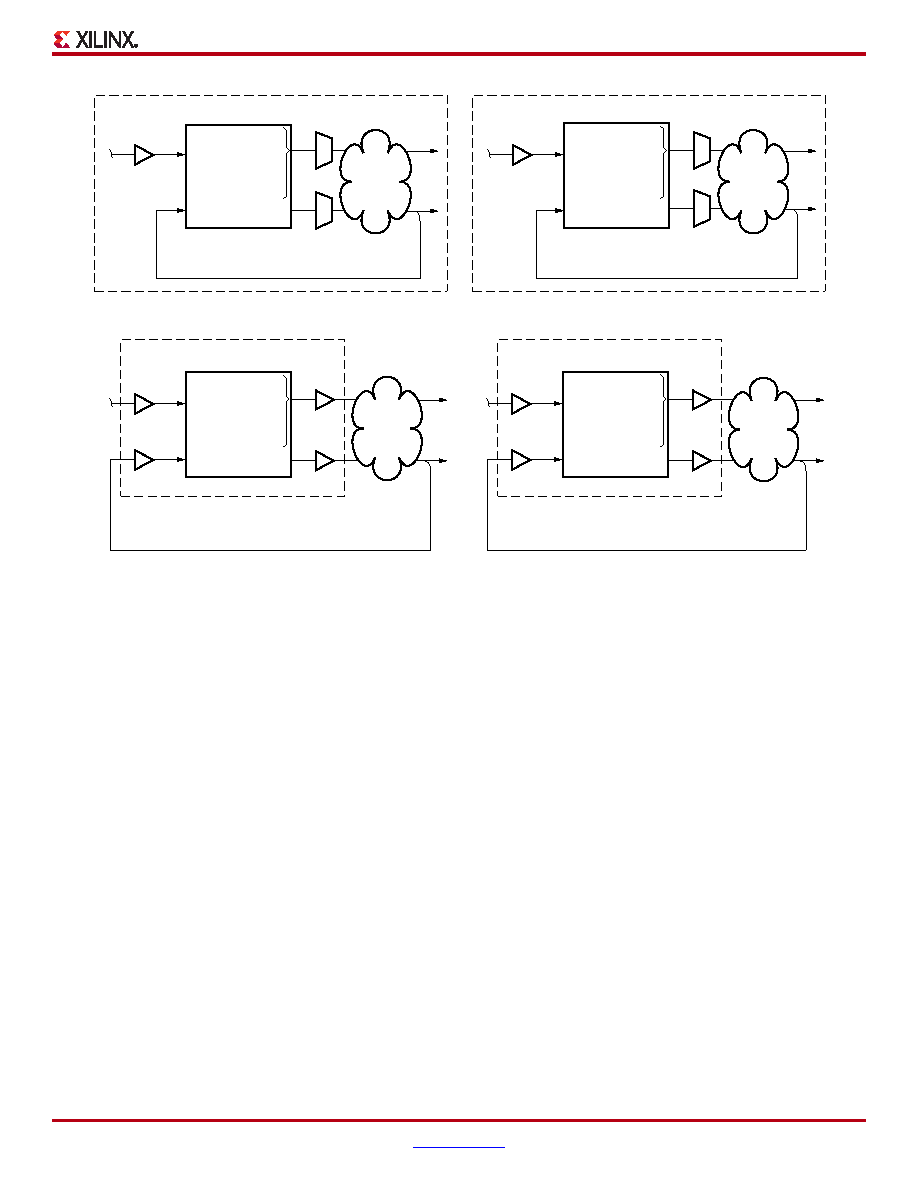
In the on-chip synchronization case (the [a] and [b] sections of Figure 21), it is possible to connect any of the DLL’s seven
output clock signals through general routing resources to the FPGA’s internal registers. Either a Global Clock Buffer (BUFG)
or a BUFGMUX affords access to the global clock network. As shown in the [a] section of Figure 21, the feedback loop is
created by routing CLK0 (or CLK2X, in the [b] section) to a global clock net, which in turn drives the CLKFB input.
In the off-chip synchronization case (the [c] and [d] sections of Figure 21), CLK0 (or CLK2X) plus any of the DLL’s other
output clock signals exit the FPGA using output buffers (OBUF) to drive an external clock network plus registers on the
board. As shown in the [c] section of Figure 21, the feedback loop is formed by feeding CLK0 (or CLK2X, in the [d] section)
back into the FPGA using an IBUFG, which directly accesses the global clock network, or an IBUF. Then, the global clock net
is connected directly to the CLKFB input.
DLL Frequency Modes
The DLL supports two distinct operating modes, High Frequency and Low Frequency, with each specified over a different
clock frequency range. The DLL_FREQUENCY_MODE attribute chooses between the two modes. When the attribute is set
to LOW, the Low Frequency mode permits all seven DLL clock outputs to operate over a low-to-moderate frequency range.
When the attribute is set to HIGH, the High Frequency mode allows the CLK0, CLK180 and CLKDV outputs to operate at the
highest possible frequencies. The remaining DLL clock outputs are not available for use in High Frequency mode.
Accommodating High Input Frequencies
If the frequency of the CLKIN signal is high such that it exceeds the maximum permitted, divide it down to an acceptable
value using the CLKIN_DIVIDE_BY_2 attribute. When this attribute is set to TRUE, the CLKIN frequency is divided by a
factor of two just as it enters the DCM.
X-Ref Target - Figure 21
Figure 21: Input Clock, Output Clock, and Feedback Connections for the DLL
DS099-2_09_082104
CLK90
CLK180
CLK270
CLKDV
CLK2X
CLK2X180
CLK0
Clock
Net Delay
BUFGMUX
BUFG
FPGA
(a) On-Chip with CLK0 Feedback
CLKIN
DCM
CLKFB
CLK90
CLK180
CLK270
CLKDV
CLK2X
CLK2X180
CLK0
Clock
Net Delay
IBUFG
FPGA
(c) Off-Chip with CLK0 Feedback
CLKIN
DCM
CLKFB
OBUF
CLK2X
IBUFG
FPGA
(d) Off-Chip with CLK2X Feedback
CLKIN
DCM
CLKFB
OBUF
CLK0
CLK90
CLK180
CLK270
CLKDV
CLK2X180
CLK2X
Clock
Net Delay
Clock
Net Delay
BUFGMUX
BUFG
FPGA
(b) On-Chip with CLK2X Feedback
CLKIN
DCM
CLKFB
CLK0
CLK90
CLK180
CLK270
CLKDV
CLK2X180
Notes:
1.
In the Low Frequency mode, all seven DLL outputs are available. In the High Frequency mode, only the CLK0, CLK180, and
CLKDV outputs are available.
相关PDF资料 |
PDF描述 |
|---|---|
| XC3S1000-5FGG676C | SPARTAN-3A FPGA 1M 676-FBGA |
| XC3S2000-4FGG900C | SPARTAN-3A FPGA 2M STD 900-FBGA |
| XA6SLX45T-3CSG324I | IC FPGA SPARTAN 6 43K 324CSGBGA |
| XA6SLX25T-2CSG324Q | IC FPGA SPARTAN 6 324CSGBGA |
| XC6SLX45T-3CSG324I | IC FPGA SPARTAN 6 43K 324CSGBGA |
相关代理商/技术参数 |
参数描述 |
|---|---|
| XC3S1000-4FT256C | 制造商:Xilinx 功能描述:FPGA SPARTAN-3 1M GATES 17280 CELLS 630MHZ 1.2V 256FTBGA - Trays 制造商:Xilinx 功能描述:IC FPGA 173 I/O 256FTBGA 制造商:Xilinx 功能描述:SPARTAN-3A FPGA 1M 256-FTBGA |
| XC3S1000-4FT256CES | 制造商:Xilinx 功能描述: |
| XC3S1000-4FT256I | 功能描述:IC FPGA SPARTAN 3 256FTBGA RoHS:否 类别:集成电路 (IC) >> 嵌入式 - FPGA(现场可编程门阵列) 系列:Spartan®-3 标准包装:40 系列:Spartan® 6 LX LAB/CLB数:3411 逻辑元件/单元数:43661 RAM 位总计:2138112 输入/输出数:358 门数:- 电源电压:1.14 V ~ 1.26 V 安装类型:表面贴装 工作温度:-40°C ~ 100°C 封装/外壳:676-BGA 供应商设备封装:676-FBGA(27x27) |
| XC3S1000-4FTG256C | 功能描述:IC SPARTAN-3 FPGA 1M 256-FTBGA RoHS:是 类别:集成电路 (IC) >> 嵌入式 - FPGA(现场可编程门阵列) 系列:Spartan®-3 标准包装:60 系列:XP LAB/CLB数:- 逻辑元件/单元数:10000 RAM 位总计:221184 输入/输出数:244 门数:- 电源电压:1.71 V ~ 3.465 V 安装类型:表面贴装 工作温度:0°C ~ 85°C 封装/外壳:388-BBGA 供应商设备封装:388-FPBGA(23x23) 其它名称:220-1241 |
| XC3S1000-4FTG256C4124 | 制造商:Xilinx 功能描述: |
发布紧急采购,3分钟左右您将得到回复。