参数资料
| 型号: | XC3S250E-4PQG208I |
| 厂商: | Xilinx Inc |
| 文件页数: | 101/227页 |
| 文件大小: | 0K |
| 描述: | IC FPGA SPARTAN-3E 250K 208-PQFP |
| 标准包装: | 24 |
| 系列: | Spartan®-3E |
| LAB/CLB数: | 612 |
| 逻辑元件/单元数: | 5508 |
| RAM 位总计: | 221184 |
| 输入/输出数: | 158 |
| 门数: | 250000 |
| 电源电压: | 1.14 V ~ 1.26 V |
| 安装类型: | 表面贴装 |
| 工作温度: | -40°C ~ 100°C |
| 封装/外壳: | 208-BFQFP |
| 供应商设备封装: | 208-PQFP(28x28) |
第1页第2页第3页第4页第5页第6页第7页第8页第9页第10页第11页第12页第13页第14页第15页第16页第17页第18页第19页第20页第21页第22页第23页第24页第25页第26页第27页第28页第29页第30页第31页第32页第33页第34页第35页第36页第37页第38页第39页第40页第41页第42页第43页第44页第45页第46页第47页第48页第49页第50页第51页第52页第53页第54页第55页第56页第57页第58页第59页第60页第61页第62页第63页第64页第65页第66页第67页第68页第69页第70页第71页第72页第73页第74页第75页第76页第77页第78页第79页第80页第81页第82页第83页第84页第85页第86页第87页第88页第89页第90页第91页第92页第93页第94页第95页第96页第97页第98页第99页第100页当前第101页第102页第103页第104页第105页第106页第107页第108页第109页第110页第111页第112页第113页第114页第115页第116页第117页第118页第119页第120页第121页第122页第123页第124页第125页第126页第127页第128页第129页第130页第131页第132页第133页第134页第135页第136页第137页第138页第139页第140页第141页第142页第143页第144页第145页第146页第147页第148页第149页第150页第151页第152页第153页第154页第155页第156页第157页第158页第159页第160页第161页第162页第163页第164页第165页第166页第167页第168页第169页第170页第171页第172页第173页第174页第175页第176页第177页第178页第179页第180页第181页第182页第183页第184页第185页第186页第187页第188页第189页第190页第191页第192页第193页第194页第195页第196页第197页第198页第199页第200页第201页第202页第203页第204页第205页第206页第207页第208页第209页第210页第211页第212页第213页第214页第215页第216页第217页第218页第219页第220页第221页第222页第223页第224页第225页第226页第227页
Spartan-3E FPGA Family: Functional Description
DS312 (v4.1) July 19, 2013
Product Specification
19
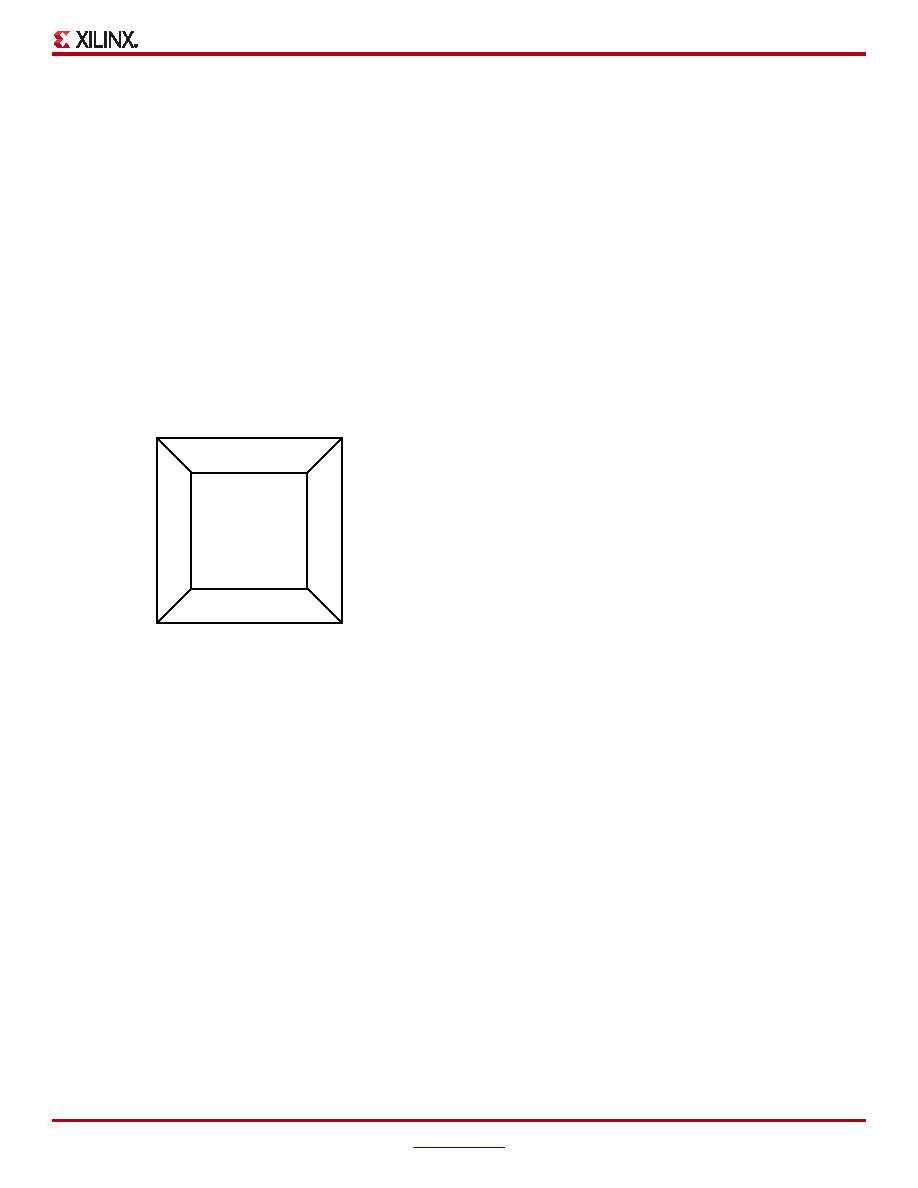
IOBs Organized into Banks
The Spartan-3E architecture organizes IOBs into four I/O
banks as shown in Figure 13. Each bank maintains
separate VCCO and VREF supplies. The separate supplies
allow each bank to independently set VCCO. Similarly, the
When working with Spartan-3E devices, most of the
differential I/O standards are compatible and can be
combined within any given bank. Each bank can support
any two of the following differential standards: LVDS_25
outputs, MINI_LVDS_25 outputs, and RSDS_25 outputs. As
an example, LVDS_25 outputs, RSDS_25 outputs, and any
other differential inputs while using on-chip differential
termination are a valid combination. A combination not
allowed is a single bank with LVDS_25 outputs, RSDS_25
outputs, and MINI_LVDS_25 outputs.
I/O Banking Rules
When assigning I/Os to banks, these VCCO rules must be
followed:
1.
All VCCO pins on the FPGA must be connected even if a
bank is unused.
2.
All VCCO lines associated within a bank must be set to
the same voltage level.
3.
The VCCO levels used by all standards assigned to the
I/Os of any given bank must agree. The Xilinx
development software checks for this. Table 6 and
Table 7 describe how different standards use the VCCO
supply.
4.
If a bank does not have any VCCO requirements,
connect VCCO to an available voltage, such as 2.5V or
3.3V. Some configuration modes might place additional
information.
If any of the standards assigned to the Inputs of the bank
use VREF, then the following additional rules must be
observed:
1.
All VREF pins must be connected within a bank.
2.
All VREF lines associated with the bank must be set to
the same voltage level.
3.
The VREF levels used by all standards assigned to the
Inputs of the bank must agree. The Xilinx development
software checks for this. Table 6 describes how different
standards use the VREF supply.
If VREF is not required to bias the input switching thresholds,
all associated VREF pins within the bank can be used as
user I/Os or input pins.
Package Footprint Compatibility
Sometimes, applications outgrow the logic capacity of a
specific Spartan-3E FPGA. Fortunately, the Spartan-3E
family is designed so that multiple part types are available in
pin-compatible package footprints, as described in
Module 4, Pinout Descriptions. In some cases, there are
subtle differences between devices available in the same
footprint. These differences are outlined for each package,
such as pins that are unconnected on one device but
connected on another in the same package or pins that are
dedicated inputs on one package but full I/O on another.
When designing the printed circuit board (PCB), plan for
potential future upgrades and package migration.
The Spartan-3E family is not pin-compatible with any
previous Xilinx FPGA family.
Dedicated Inputs
Dedicated Inputs are IOBs used only as inputs. Pin names
designate a Dedicated Input if the name starts with IP, for
example, IP or IP_Lxxx_x. Dedicated inputs retain the full
functionality of the IOB for input functions with a single
exception for differential inputs (IP_Lxxx_x). For the
differential Dedicated Inputs, the on-chip differential
termination is not available. To replace the on-chip
differential termination, choose a differential pair that
supports outputs (IO_Lxxx_x) or use an external 100
Ω
termination resistor on the board.
ESD Protection
Clamp diodes protect all device pads against damage from
Electro-Static Discharge (ESD) as well as excessive voltage
transients. Each I/O has two clamp diodes: one diode
extends P-to-N from the pad to VCCO and a second diode
extends N-to-P from the pad to GND. During operation,
these diodes are normally biased in the off state. These
clamp diodes are always connected to the pad, regardless
of the signal standard selected. The presence of diodes
limits the ability of Spartan-3E I/Os to tolerate high signal
Module 3, DC and Switching Characteristics specifies the
voltage range that I/Os can tolerate.
X-Ref Target - Figure 13
Figure 13: Spartan-3E I/O Banks (top view)
DS312-2_26_021205
Bank 0
Bank 2
Bank
3
Bank
1
相关PDF资料 |
PDF描述 |
|---|---|
| AYM43DRST-S288 | CONN EDGECARD 86POS .156 EXTEND |
| XC3S200A-5FGG320C | IC SPARTAN-3A FPGA 200K 320-FBGA |
| 93LC76CT-I/ST | IC EEPROM 8KBIT 3MHZ 8TSSOP |
| EHHD15MM | CONN DSUB 15PIN MALE-MALE |
| ASM43DRST-S288 | CONN EDGECARD 86POS .156 EXTEND |
相关代理商/技术参数 |
参数描述 |
|---|---|
| XC3S250E-4TQ144C | 制造商:Xilinx 功能描述:FPGA SPARTAN-3E 250K GATES 5508 CELLS 572MHZ 90NM 1.2V 144TQ - Trays |
| XC3S250E-4TQ144I | 功能描述:IC FPGA SPARTAN 3E 144TQFP RoHS:否 类别:集成电路 (IC) >> 嵌入式 - FPGA(现场可编程门阵列) 系列:Spartan®-3E 标准包装:40 系列:Spartan® 6 LX LAB/CLB数:3411 逻辑元件/单元数:43661 RAM 位总计:2138112 输入/输出数:358 门数:- 电源电压:1.14 V ~ 1.26 V 安装类型:表面贴装 工作温度:-40°C ~ 100°C 封装/外壳:676-BGA 供应商设备封装:676-FBGA(27x27) |
| XC3S250E-4TQG144C | 功能描述:IC SPARTAN-3E FPGA 250K 144TQFP RoHS:是 类别:集成电路 (IC) >> 嵌入式 - FPGA(现场可编程门阵列) 系列:Spartan®-3E 标准包装:60 系列:XP LAB/CLB数:- 逻辑元件/单元数:10000 RAM 位总计:221184 输入/输出数:244 门数:- 电源电压:1.71 V ~ 3.465 V 安装类型:表面贴装 工作温度:0°C ~ 85°C 封装/外壳:388-BBGA 供应商设备封装:388-FPBGA(23x23) 其它名称:220-1241 |
| XC3S250E-4TQG144I | 功能描述:IC FPGA SPARTAN-3E 250K 144-TQFP RoHS:是 类别:集成电路 (IC) >> 嵌入式 - FPGA(现场可编程门阵列) 系列:Spartan®-3E 标准包装:40 系列:Spartan® 6 LX LAB/CLB数:3411 逻辑元件/单元数:43661 RAM 位总计:2138112 输入/输出数:358 门数:- 电源电压:1.14 V ~ 1.26 V 安装类型:表面贴装 工作温度:-40°C ~ 100°C 封装/外壳:676-BGA 供应商设备封装:676-FBGA(27x27) |
| XC3S250E-4VQ100C | 制造商:Xilinx 功能描述:FPGA SPARTAN-3E 250K GATES 5508 CELLS 572MHZ 90NM 1.2V 100VT - Trays |
发布紧急采购,3分钟左右您将得到回复。