参数资料
| 型号: | XC4013E-4PQ240I |
| 厂商: | Xilinx Inc |
| 文件页数: | 15/68页 |
| 文件大小: | 0K |
| 描述: | IC FPGA I-TEMP 5V 4SPD 240-PQFP |
| 产品变化通告: | Product Discontinuation 28/Jul/2010 |
| 标准包装: | 24 |
| 系列: | XC4000E/X |
| LAB/CLB数: | 576 |
| 逻辑元件/单元数: | 1368 |
| RAM 位总计: | 18432 |
| 输入/输出数: | 192 |
| 门数: | 13000 |
| 电源电压: | 4.5 V ~ 5.5 V |
| 安装类型: | 表面贴装 |
| 工作温度: | -40°C ~ 100°C |
| 封装/外壳: | 240-BFQFP |
| 供应商设备封装: | 240-PQFP(32x32) |
第1页第2页第3页第4页第5页第6页第7页第8页第9页第10页第11页第12页第13页第14页当前第15页第16页第17页第18页第19页第20页第21页第22页第23页第24页第25页第26页第27页第28页第29页第30页第31页第32页第33页第34页第35页第36页第37页第38页第39页第40页第41页第42页第43页第44页第45页第46页第47页第48页第49页第50页第51页第52页第53页第54页第55页第56页第57页第58页第59页第60页第61页第62页第63页第64页第65页第66页第67页第68页
R
XC4000E and XC4000X Series Field Programmable Gate Arrays
6-26
May 14, 1999 (Version 1.6)
or clear on reset and after conguration. Other than the glo-
bal GSR net, no user-controlled set/reset signal is available
to the I/O ip-ops. The choice of set or clear applies to
both the initial state of the ip-op and the response to the
Global Set/Reset pulse. See “Global Set/Reset” on
page 11 for a description of how to use GSR.
JTAG Support
Embedded logic attached to the IOBs contains test struc-
tures compatible with IEEE Standard 1149.1 for boundary
scan testing, permitting easy chip and board-level testing.
More information is provided in “Boundary Scan” on
Three-State Buffers
A pair of 3-state buffers is associated with each CLB in the
array. (See Figure 27 on page 30.) These 3-state buffers
can be used to drive signals onto the nearest horizontal
longlines above and below the CLB. They can therefore be
used to implement multiplexed or bidirectional buses on the
horizontal longlines, saving logic resources. Programmable
pull-up resistors attached to these longlines help to imple-
ment a wide wired-AND function.
The buffer enable is an active-High 3-state (i.e. an
active-Low enable), as shown in Table 13.
Another 3-state buffer with similar access is located near
each I/O block along the right and left edges of the array.
(See Figure 33 on page 34.)
The horizontal longlines driven by the 3-state buffers have
a weak keeper at each end. This circuit prevents undened
oating levels. However, it is overridden by any driver, even
a pull-up resistor.
Special longlines running along the perimeter of the array
can be used to wire-AND signals coming from nearby IOBs
or from internal longlines. These longlines form the wide
edge decoders discussed in “Wide Edge Decoders” on
Three-State Buffer Modes
The 3-state buffers can be congured in three modes:
Standard 3-state buffer
Wired-AND with input on the I pin
Wired OR-AND
Standard 3-State Buffer
All three pins are used. Place the library element BUFT.
Connect the input to the I pin and the output to the O pin.
The T pin is an active-High 3-state (i.e. an active-Low
enable). Tie the T pin to Ground to implement a standard
buffer.
Wired-AND with Input on the I Pin
The buffer can be used as a Wired-AND. Use the WAND1
library symbol, which is essentially an open-drain buffer.
WAND4, WAND8, and WAND16 are also available. See the
XACT Libraries Guide for further information.
The T pin is internally tied to the I pin. Connect the input to
the I pin and the output to the O pin. Connect the outputs of
all the WAND1s together and attach a PULLUP symbol.
Wired OR-AND
The buffer can be congured as a Wired OR-AND. A High
level on either input turns off the output. Use the
WOR2AND library symbol, which is essentially an
open-drain 2-input OR gate. The two input pins are func-
tionally equivalent. Attach the two inputs to the I0 and I1
pins and tie the output to the O pin. Tie the outputs of all the
WOR2ANDs together and attach a PULLUP symbol.
Three-State Buffer Examples
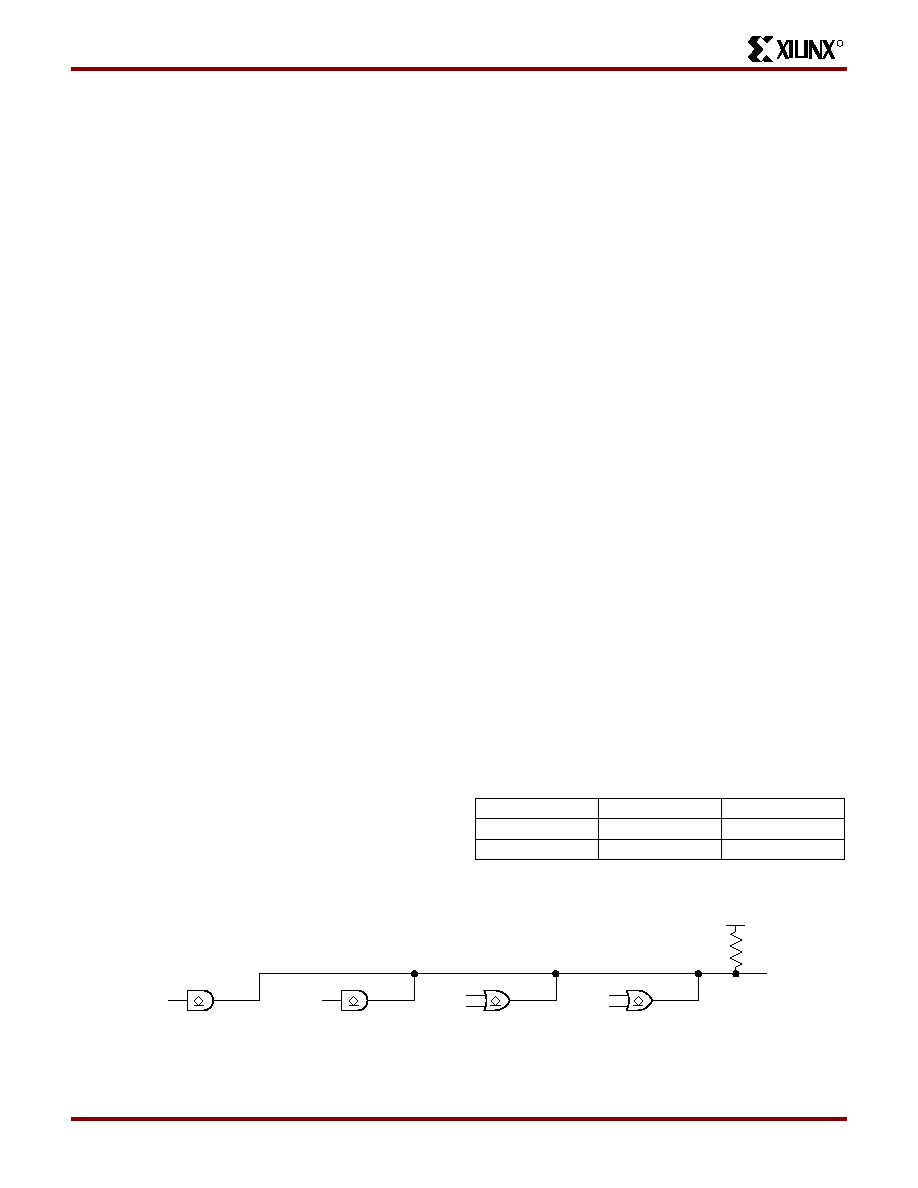
Figure 21 shows how to use the 3-state buffers to imple-
ment a wired-AND function. When all the buffer inputs are
High, the pull-up resistor(s) provide the High output.
Figure 22 shows how to use the 3-state buffers to imple-
ment a multiplexer. The selection is accomplished by the
buffer 3-state signal.
Pay particular attention to the polarity of the T pin when
using these buffers in a design. Active-High 3-state (T) is
identical to an active-Low output enable, as shown in
Table 13: Three-State Buffer Functionality
IN
T
OUT
X1
Z
IN
0
IN
P
U
L
U
P
Z = D
A
q
D
B
q
(D
C
+D
D
) q (D
E
+D
F
)
D
E
D
F
D
C
D
B
D
A
WAND1
WOR2AND
X6465
Figure 21: Open-Drain Buffers Implement a Wired-AND Function
Product Obsolete or Under Obsolescence
相关PDF资料 |
PDF描述 |
|---|---|
| XC4013E-4PQ240C | IC FPGA C-TEMP 5V 4SPD 240-PQFP |
| AMM36DRSI-S288 | CONN EDGECARD 72POS .156 EXTEND |
| IDT71V35761S200BGG8 | IC SRAM 4MBIT 200MHZ 119BGA |
| FMM28DSEF-S13 | CONN EDGECARD 56POS .156 EXTEND |
| IDT71V35761S200BG8 | IC SRAM 4MBIT 200MHZ 119BGA |
相关代理商/技术参数 |
参数描述 |
|---|---|
| XC4013E-4PQ240M | 制造商:XILINX 制造商全称:XILINX 功能描述:Programmable Gate Arrays |
| XC4013E-4TQ240C | 制造商:XILINX 制造商全称:XILINX 功能描述:XC4000E and XC4000X Series Field Programmable Gate Arrays |
| XC4013E-4TQ240I | 制造商:XILINX 制造商全称:XILINX 功能描述:XC4000E and XC4000X Series Field Programmable Gate Arrays |
| XC4013E-4TQ240M | 制造商:XILINX 制造商全称:XILINX 功能描述:XC4000E and XC4000X Series Field Programmable Gate Arrays |
| XC4013E-4VQ240C | 制造商:XILINX 制造商全称:XILINX 功能描述:XC4000E and XC4000X Series Field Programmable Gate Arrays |
发布紧急采购,3分钟左右您将得到回复。