参数资料
| 型号: | XC4020XL-3PQ240I |
| 厂商: | Xilinx Inc |
| 文件页数: | 31/68页 |
| 文件大小: | 0K |
| 描述: | IC FPGA I-TEMP 3.3V 3SPD 240PQFP |
| 产品变化通告: | XC4000XL/E, XC9500XV, XC3100A Discontinuance 12/Apr/2010 |
| 标准包装: | 1 |
| 系列: | XC4000E/X |
| LAB/CLB数: | 784 |
| 逻辑元件/单元数: | 1862 |
| RAM 位总计: | 25088 |
| 输入/输出数: | 192 |
| 门数: | 20000 |
| 电源电压: | 3 V ~ 3.6 V |
| 安装类型: | 表面贴装 |
| 工作温度: | -40°C ~ 100°C |
| 封装/外壳: | 240-BFQFP |
| 供应商设备封装: | 240-PQFP(32x32) |
第1页第2页第3页第4页第5页第6页第7页第8页第9页第10页第11页第12页第13页第14页第15页第16页第17页第18页第19页第20页第21页第22页第23页第24页第25页第26页第27页第28页第29页第30页当前第31页第32页第33页第34页第35页第36页第37页第38页第39页第40页第41页第42页第43页第44页第45页第46页第47页第48页第49页第50页第51页第52页第53页第54页第55页第56页第57页第58页第59页第60页第61页第62页第63页第64页第65页第66页第67页第68页
R
May 14, 1999 (Version 1.6)
6-41
XC4000E and XC4000X Series Field Programmable Gate Arrays
6
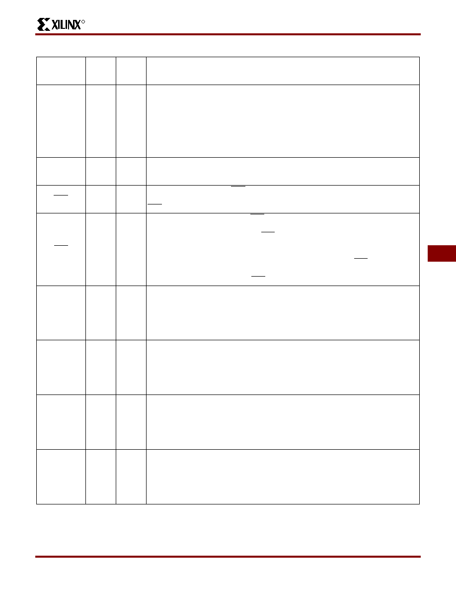
TDI, TCK,
TMS
I
I/O
or I
(JTAG)
If boundary scan is used, these pins are Test Data In, Test Clock, and Test Mode Select
inputs respectively. They come directly from the pads, bypassing the IOBs. These pins
can also be used as inputs to the CLB logic after configuration is completed.
If the BSCAN symbol is not placed in the design, all boundary scan functions are inhib-
ited once configuration is completed, and these pins become user-programmable I/O.
The pins can be used automatically or user-constrained. To use them, use "LOC=" or
place the library components TDI, TCK, and TMS instead of the usual pad symbols. In-
put or output buffers must still be used.
HDC
O
I/O
High During Configuration (HDC) is driven High until the I/O go active. It is available as
a control output indicating that configuration is not yet completed. After configuration,
HDC is a user-programmable I/O pin.
LDC
O
I/O
Low During Configuration (LDC) is driven Low until the I/O go active. It is available as a
control output indicating that configuration is not yet completed. After configuration,
LDC is a user-programmable I/O pin.
INIT
I/O
Before and during configuration, INIT is a bidirectional signal. A 1 k
- 10 k external
pull-up resistor is recommended.
As an active-Low open-drain output, INIT is held Low during the power stabilization and
internal clearing of the configuration memory. As an active-Low input, it can be used
to hold the FPGA in the internal WAIT state before the start of configuration. Master
mode devices stay in a WAIT state an additional 30 to 300
s after INIT has gone High.
During configuration, a Low on this output indicates that a configuration data error has
occurred. After the I/O go active, INIT is a user-programmable I/O pin.
PGCK1 -
PGCK4
(XC4000E
only)
Weak
Pull-up
I or I/O
Four Primary Global inputs each drive a dedicated internal global net with short delay
and minimal skew. If not used to drive a global buffer, any of these pins is a user-pro-
grammable I/O.
The PGCK1-PGCK4 pins drive the four Primary Global Buffers. Any input pad symbol
connected directly to the input of a BUFGP symbol is automatically placed on one of
these pins.
SGCK1 -
SGCK4
(XC4000E
only)
Weak
Pull-up
I or I/O
Four Secondary Global inputs each drive a dedicated internal global net with short delay
and minimal skew. These internal global nets can also be driven from internal logic. If
not used to drive a global net, any of these pins is a user-programmable I/O pin.
The SGCK1-SGCK4 pins provide the shortest path to the four Secondary Global Buff-
ers. Any input pad symbol connected directly to the input of a BUFGS symbol is auto-
matically placed on one of these pins.
GCK1 -
GCK8
(XC4000X
only)
Weak
Pull-up
I or I/O
Eight inputs can each drive a Global Low-Skew buffer. In addition, each can drive a Glo-
bal Early buffer. Each pair of global buffers can also be driven from internal logic, but
must share an input signal. If not used to drive a global buffer, any of these pins is a
user-programmable I/O.
Any input pad symbol connected directly to the input of a BUFGLS or BUFGE symbol
is automatically placed on one of these pins.
FCLK1 -
FCLK4
(XC4000XLA
and
XC4000XV
only)
Weak
Pull-up
I or I/O
Four inputs can each drive a Fast Clock (FCLK) buffer which can deliver a clock signal
to any IOB clock input in the octant of the die served by the Fast Clock buffer. Two Fast
Clock buffers serve the two IOB octants on the left side of the die and the other two Fast
Clock buffers serve the two IOB octants on the right side of the die. On each side of the
die, one Fast Clock buffer serves the upper octant and the other serves the lower octant.
If not used to drive a Fast Clock buffer, any of these pins is a user-programmable I/O.
Table 16: Pin Descriptions (Continued)
Pin Name
I/O
During
Cong.
I/O
After
Cong.
Pin Description
Product Obsolete or Under Obsolescence
相关PDF资料 |
PDF描述 |
|---|---|
| XC4020XL-3PQ240C | IC FPGA C-TEMP 3.3V 3SPD 240PQFP |
| ABB106DHBT-S621 | CONN EDGECARD 212PS R/A .050 SLD |
| ACB106DHBT-S621 | EDGECARD 212POS DIP R/A .050 SLD |
| MC8641DTVU1333JE | IC MPU DUAL CORE E600 1023FCCBGA |
| MC7457TRX1000NC | IC MPU RISC 32BIT 483FCCBGA |
相关代理商/技术参数 |
参数描述 |
|---|---|
| XC4020XLA-07PQ160C | 制造商:Xilinx 功能描述: |
| XC4020XLA-08BG256C | 制造商:Rochester Electronics LLC 功能描述: 制造商:Xilinx 功能描述:FPGA, 784 CLBS, 13000 GATES, 263 MHz, 256 Pin Plastic BGA |
| XC4020XLA-09BG256C | 制造商:Rochester Electronics LLC 功能描述: 制造商:Xilinx 功能描述: |
| XC4020XLA09C-BG256AKP | 制造商:Xilinx 功能描述: |
| XC4020XLA-09PQ160C | 制造商:Xilinx 功能描述: |
发布紧急采购,3分钟左右您将得到回复。