参数资料
| 型号: | XC4020XL-3PQ240I |
| 厂商: | Xilinx Inc |
| 文件页数: | 41/68页 |
| 文件大小: | 0K |
| 描述: | IC FPGA I-TEMP 3.3V 3SPD 240PQFP |
| 产品变化通告: | XC4000XL/E, XC9500XV, XC3100A Discontinuance 12/Apr/2010 |
| 标准包装: | 1 |
| 系列: | XC4000E/X |
| LAB/CLB数: | 784 |
| 逻辑元件/单元数: | 1862 |
| RAM 位总计: | 25088 |
| 输入/输出数: | 192 |
| 门数: | 20000 |
| 电源电压: | 3 V ~ 3.6 V |
| 安装类型: | 表面贴装 |
| 工作温度: | -40°C ~ 100°C |
| 封装/外壳: | 240-BFQFP |
| 供应商设备封装: | 240-PQFP(32x32) |
第1页第2页第3页第4页第5页第6页第7页第8页第9页第10页第11页第12页第13页第14页第15页第16页第17页第18页第19页第20页第21页第22页第23页第24页第25页第26页第27页第28页第29页第30页第31页第32页第33页第34页第35页第36页第37页第38页第39页第40页当前第41页第42页第43页第44页第45页第46页第47页第48页第49页第50页第51页第52页第53页第54页第55页第56页第57页第58页第59页第60页第61页第62页第63页第64页第65页第66页第67页第68页
R
XC4000E and XC4000X Series Field Programmable Gate Arrays
6-50
May 14, 1999 (Version 1.6)
used), and if RAM is present, the RAM content must be
unchanged.
Statistically, one error out of 2048 might go undetected.
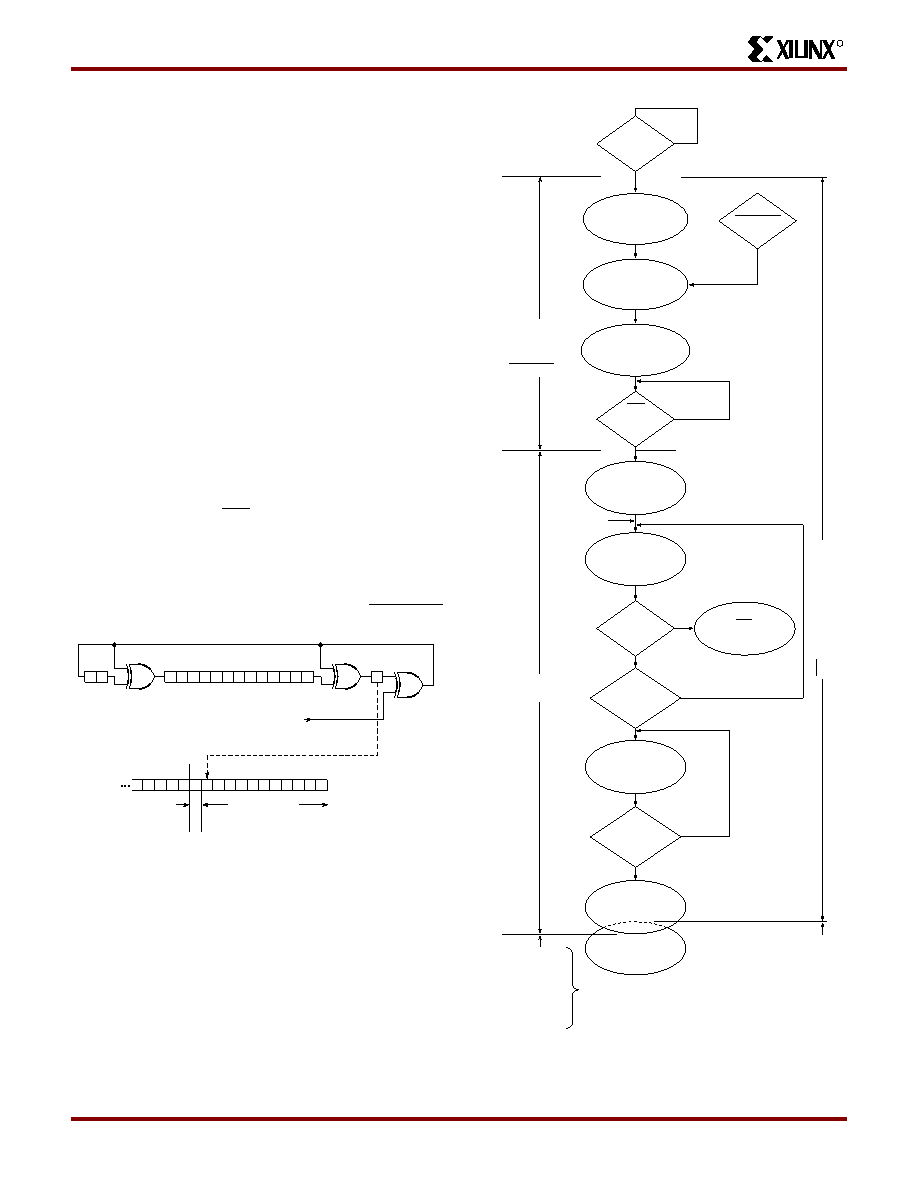
Conguration Sequence
There are four major steps in the XC4000 Series power-up
conguration sequence.
Conguration Memory Clear
Initialization
Conguration
Start-Up
The full process is illustrated in Figure 46.
Conguration Memory Clear
When power is rst applied or is reapplied to an FPGA, an
internal circuit forces initialization of the conguration logic.
When Vcc reaches an operational level, and the circuit
passes the write and read test of a sample pair of congu-
ration bits, a time delay is started. This time delay is nomi-
nally 16 ms, and up to 10% longer in the low-voltage
devices. The delay is four times as long when in Master
Modes (M0 Low), to allow ample time for all slaves to reach
a stable Vcc. When all INIT pins are tied together, as rec-
ommended, the longest delay takes precedence. There-
fore, devices with different time delays can easily be mixed
and matched in a daisy chain.
This delay is applied only on power-up. It is not applied
when re-conguring an FPGA by pulsing the PROGRAM
pin
0
X2
2 3456789 10 11 12 13 14
1
X15
X16
15
SERIAL DATA IN
1 0 1514 13 12 1110 9 8 7 65
1
CRC – CHECKSUM
LAST DATA FRAME
START
BIT
X1789
Polynomial: X16 + X15 + X2 + 1
Readback Data Stream
Figure 45: Circuit for Generating CRC-16
INIT
High? if
Master
Sample
Mode Lines
Load One
Configuration
Data Frame
Frame
Error
Pass
Configuration
Data to DOUT
VCC
>3.5 V
No
Yes
No
Yes
Operational
Start-Up
Sequence
No
Yes
~1.3
s per Frame
Master Waits 50 to 250
s
Before Sampling Mode Lines
Master CCLK
Goes Active
F
Pull INIT Low
and Stop
X6076
EXTEST*
SAMPLE/PRELOAD
BYPASS
CONFIGURE*
(* if PROGRAM = High)
SAMPLE/PRELOAD
BYPASS
EXTEST
SAMPLE PRELOAD
BYPASS
USER 1
USER 2
CONFIGURE
READBACK
If Boundary Scan
is Selected
Config-
uration
memory
Full
CCLK
Count Equals
Length
Count
Completely Clear
Configuration Memory
Once More
LDC
Output
=
L,
HDC
Output
=
H
Boundary Scan
Instructions
Available:
I/O
Active
Keep Clearing
Configuration Memory
Test M0 Generate
One Time-Out Pulse
of 16 or 64 ms
PROGRAM
= Low
No
Yes
Figure 46: Power-up Conguration Sequence
Product Obsolete or Under Obsolescence
相关PDF资料 |
PDF描述 |
|---|---|
| XC4020XL-3PQ240C | IC FPGA C-TEMP 3.3V 3SPD 240PQFP |
| ABB106DHBT-S621 | CONN EDGECARD 212PS R/A .050 SLD |
| ACB106DHBT-S621 | EDGECARD 212POS DIP R/A .050 SLD |
| MC8641DTVU1333JE | IC MPU DUAL CORE E600 1023FCCBGA |
| MC7457TRX1000NC | IC MPU RISC 32BIT 483FCCBGA |
相关代理商/技术参数 |
参数描述 |
|---|---|
| XC4020XLA-07PQ160C | 制造商:Xilinx 功能描述: |
| XC4020XLA-08BG256C | 制造商:Rochester Electronics LLC 功能描述: 制造商:Xilinx 功能描述:FPGA, 784 CLBS, 13000 GATES, 263 MHz, 256 Pin Plastic BGA |
| XC4020XLA-09BG256C | 制造商:Rochester Electronics LLC 功能描述: 制造商:Xilinx 功能描述: |
| XC4020XLA09C-BG256AKP | 制造商:Xilinx 功能描述: |
| XC4020XLA-09PQ160C | 制造商:Xilinx 功能描述: |
发布紧急采购,3分钟左右您将得到回复。