参数资料
| 型号: | XC6SLX75T-3FG676I |
| 厂商: | Xilinx Inc |
| 文件页数: | 30/89页 |
| 文件大小: | 0K |
| 描述: | IC FPGA SPARTAN 6 676FGGBGA |
| 标准包装: | 40 |
| 系列: | Spartan® 6 LXT |
| LAB/CLB数: | 5831 |
| 逻辑元件/单元数: | 74637 |
| RAM 位总计: | 3170304 |
| 输入/输出数: | 348 |
| 电源电压: | 1.14 V ~ 1.26 V |
| 安装类型: | 表面贴装 |
| 工作温度: | -40°C ~ 100°C |
| 封装/外壳: | 676-BGA |
| 供应商设备封装: | 676-FBGA(27x27) |
第1页第2页第3页第4页第5页第6页第7页第8页第9页第10页第11页第12页第13页第14页第15页第16页第17页第18页第19页第20页第21页第22页第23页第24页第25页第26页第27页第28页第29页当前第30页第31页第32页第33页第34页第35页第36页第37页第38页第39页第40页第41页第42页第43页第44页第45页第46页第47页第48页第49页第50页第51页第52页第53页第54页第55页第56页第57页第58页第59页第60页第61页第62页第63页第64页第65页第66页第67页第68页第69页第70页第71页第72页第73页第74页第75页第76页第77页第78页第79页第80页第81页第82页第83页第84页第85页第86页第87页第88页第89页
Spartan-6 FPGA Data Sheet: DC and Switching Characteristics
DS162 (v3.0) October 17, 2011
Product Specification
36
Simultaneously Switching Outputs
Due to package electrical parasitics, a given package supports a limited number of simultaneous switching outputs (SSOs)
when using fast, high-drive outputs. Table 33 and Table 34 provide guidelines for the recommended maximum allowable
number of SSOs. These guidelines describe the maximum number of user I/O pins of an output signal standard that should
simultaneously switch in the same direction, while maintaining a safe level of switching noise for that particular signal
standard. Meeting these guidelines for the stated test conditions ensures that the FPGA operates free from the adverse
effects of GND and power bounce.
For each device/package combination, Table 33 provides the number of equivalent VCCO/GND pairs per bank. For each
output signal standard and drive strength, Table 34 recommends the maximum number of SSOs, switching in the same
direction, allowed per VCCO/GND pair within an I/O bank. The guidelines are categorized by package style, slew rate, and
output drive current. The number of SSOs are also specified by I/O bank. Multiply the appropriate numbers from each table
to calculate the maximum number of SSOs allowed within an I/O bank. The guidelines assume that all pins within a bank use
the same I/O standard. Exceeding these SSO guidelines can result in increased power or GND bounce, degraded signal
integrity, or increased system jitter. For a given I/O standard, if the SSO limit per pair in Table 34 is greater than the maximum
I/O per pair in Table 33, then there is no SSO limit for the exclusive use of that I/O standard.
The recommended maximum SSO values assume that the FPGA is soldered on a printed circuit board and that the board
uses sound design practices. Due to the additional inductance introduced by the socket, the SSO values do not apply for
FPGAs mounted in sockets. The SSO values assume that the VCCAUX is powered at 3.3V. Setting VCCAUX to 2.5V provides
better SSO characteristics. For more detail, see UG381: Spartan-6 FPGA SelectIO Resources User Guide.
SSTL, Class II, 2.5V
SSTL2_II
25
0
VREF
1.25
SSTL, Class II, 1.5V
SSTL15_II
25
0
VREF
0.75
LVDS (Low-Voltage Differential Signaling), 2.5V & 3.3V
LVDS_25, LVDS_33
100
0
–
BLVDS (Bus LVDS), 2.5V
BLVDS_25
–
Mini-LVDS, 2.5V & 3.3V
MINI_LVDS_25, MINI_LVDS_33
100
0
0(3)
–
RSDS (Reduced Swing Differential Signaling), 2.5V & 3.3V RSDS_25, RSDS_33
100
0
0(3)
–
TMDS (Transition Minimized Differential Signaling), 3.3V
TMDS_33
–
PPDS (Point-to-Point Differential Signaling, 2.5V & 3.3V
PPDS_25, PPDS_33
100
0
–
Notes:
1.
CREF is the capacitance of the probe, nominally 0 pF.
2.
Per PCI specifications.
3.
The value given is the differential output voltage.
4.
See the BLVDS Output Termination section in UG381, Spartan-6 FPGA SelectIO Resources User Guide.
5.
See the TMDS_33 Termination section in UG381, Spartan-6 FPGA SelectIO Resources User Guide.
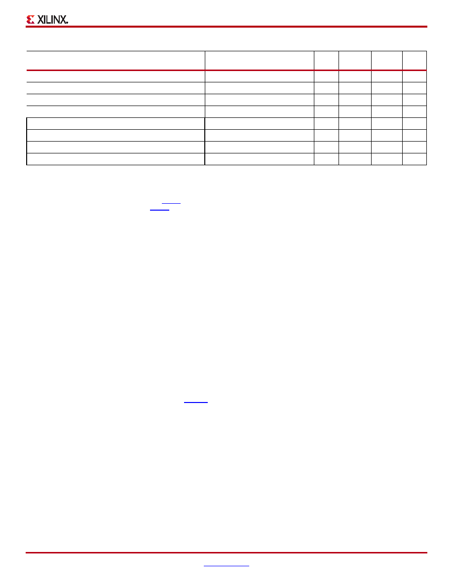
Table 32: Output Delay Measurement Methodology (Cont’d)
Description
I/O Standard
Attribute
RREF
(
)
CREF(1)
(pF)
VMEAS
(V)
VREF
(V)
相关PDF资料 |
PDF描述 |
|---|---|
| 25LC128T-E/SM | IC EEPROM 128KBIT 10MHZ 8SOIC |
| XC6SLX75T-3FGG676I | IC FPGA SPARTAN 6 74K 676FGGBGA |
| 25LC128-E/SN | IC EEPROM 128KBIT 10MHZ 8SOIC |
| AMC30DRYS-S734 | CONN EDGECARD 60POS DIP .100 SLD |
| 12600-S-10 | THUMBSCREW LOCK SDR SHELL 0.18" |
相关代理商/技术参数 |
参数描述 |
|---|---|
| XC6SLX75T-3FGG484C | 功能描述:IC FPGA SPARTAN 6 74K 484FGGBGA RoHS:是 类别:集成电路 (IC) >> 嵌入式 - FPGA(现场可编程门阵列) 系列:Spartan® 6 LXT 产品变化通告:Step Intro and Pkg Change 11/March/2008 标准包装:1 系列:Virtex®-5 SXT LAB/CLB数:4080 逻辑元件/单元数:52224 RAM 位总计:4866048 输入/输出数:480 门数:- 电源电压:0.95 V ~ 1.05 V 安装类型:表面贴装 工作温度:-40°C ~ 100°C 封装/外壳:1136-BBGA,FCBGA 供应商设备封装:1136-FCBGA 配用:568-5088-ND - BOARD DEMO DAC1408D750122-1796-ND - EVALUATION PLATFORM VIRTEX-5 |
| XC6SLX75T-3FGG484I | 功能描述:IC FPGA SPARTAN 6 74K 484FGGBGA RoHS:是 类别:集成电路 (IC) >> 嵌入式 - FPGA(现场可编程门阵列) 系列:Spartan® 6 LXT 产品变化通告:Step Intro and Pkg Change 11/March/2008 标准包装:1 系列:Virtex®-5 SXT LAB/CLB数:4080 逻辑元件/单元数:52224 RAM 位总计:4866048 输入/输出数:480 门数:- 电源电压:0.95 V ~ 1.05 V 安装类型:表面贴装 工作温度:-40°C ~ 100°C 封装/外壳:1136-BBGA,FCBGA 供应商设备封装:1136-FCBGA 配用:568-5088-ND - BOARD DEMO DAC1408D750122-1796-ND - EVALUATION PLATFORM VIRTEX-5 |
| XC6SLX75T-3FGG676C | 功能描述:IC FPGA SPARTAN 6 74K 676FGGBGA RoHS:是 类别:集成电路 (IC) >> 嵌入式 - FPGA(现场可编程门阵列) 系列:Spartan® 6 LXT 产品变化通告:Step Intro and Pkg Change 11/March/2008 标准包装:1 系列:Virtex®-5 SXT LAB/CLB数:4080 逻辑元件/单元数:52224 RAM 位总计:4866048 输入/输出数:480 门数:- 电源电压:0.95 V ~ 1.05 V 安装类型:表面贴装 工作温度:-40°C ~ 100°C 封装/外壳:1136-BBGA,FCBGA 供应商设备封装:1136-FCBGA 配用:568-5088-ND - BOARD DEMO DAC1408D750122-1796-ND - EVALUATION PLATFORM VIRTEX-5 |
| XC6SLX75T-3FGG676I | 功能描述:IC FPGA SPARTAN 6 74K 676FGGBGA RoHS:是 类别:集成电路 (IC) >> 嵌入式 - FPGA(现场可编程门阵列) 系列:Spartan® 6 LXT 产品变化通告:Step Intro and Pkg Change 11/March/2008 标准包装:1 系列:Virtex®-5 SXT LAB/CLB数:4080 逻辑元件/单元数:52224 RAM 位总计:4866048 输入/输出数:480 门数:- 电源电压:0.95 V ~ 1.05 V 安装类型:表面贴装 工作温度:-40°C ~ 100°C 封装/外壳:1136-BBGA,FCBGA 供应商设备封装:1136-FCBGA 配用:568-5088-ND - BOARD DEMO DAC1408D750122-1796-ND - EVALUATION PLATFORM VIRTEX-5 |
| XC6SLX75T-4CSG484C | 功能描述:IC FPGA SPARTAN 6 74K 484CSGBGA RoHS:是 类别:集成电路 (IC) >> 嵌入式 - FPGA(现场可编程门阵列) 系列:Spartan® 6 LXT 标准包装:1 系列:Kintex-7 LAB/CLB数:25475 逻辑元件/单元数:326080 RAM 位总计:16404480 输入/输出数:350 门数:- 电源电压:0.97 V ~ 1.03 V 安装类型:表面贴装 工作温度:0°C ~ 85°C 封装/外壳:900-BBGA,FCBGA 供应商设备封装:900-FCBGA(31x31) 其它名称:122-1789 |
发布紧急采购,3分钟左右您将得到回复。