- 您现在的位置:买卖IC网 > PDF目录19909 > XCF02SVO20C (Xilinx Inc)IC PROM IN SYST PRG 3.3V 20TSSOP PDF资料下载
参数资料
| 型号: | XCF02SVO20C |
| 厂商: | Xilinx Inc |
| 文件页数: | 5/35页 |
| 文件大小: | 0K |
| 描述: | IC PROM IN SYST PRG 3.3V 20TSSOP |
| 标准包装: | 74 |
| 可编程类型: | 系统内可编程 |
| 存储容量: | 2Mb |
| 电源电压: | 3 V ~ 3.6 V |
| 工作温度: | -40°C ~ 85°C |
| 封装/外壳: | 20-TSSOP(0.173",4.40mm 宽) |
| 供应商设备封装: | 20-TSSOP |
| 包装: | 管件 |
第1页第2页第3页第4页当前第5页第6页第7页第8页第9页第10页第11页第12页第13页第14页第15页第16页第17页第18页第19页第20页第21页第22页第23页第24页第25页第26页第27页第28页第29页第30页第31页第32页第33页第34页第35页
Platform Flash In-System Programmable Configuration PROMs
DS123 (v2.18) May 19, 2010
Product Specification
13
R
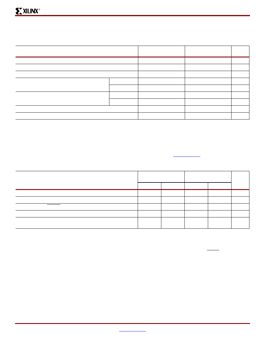
DC Electrical Characteristics
Absolute Maximum Ratings
Supply Voltage Requirements for Power-On Reset and Power-Down
Symbol
Description
XCF01S, XCF02S,
XCF04S
XCF08P, XCF16P,
XCF32P
Units
VCCINT
Internal supply voltage relative to GND
–0.5 to +4.0
–0.5 to +2.7
V
VCCO
I/O supply voltage relative to GND
–0.5 to +4.0
V
VCCJ
JTAG I/O supply voltage relative to GND
–0.5 to +4.0
V
VIN
Input voltage with respect to GND
VCCO < 2.5V
–0.5 to +3.6
V
VCCO ≥ 2.5V
–0.5 to +5.5
–0.5 to +3.6
V
VTS
Voltage applied to High-Z output
VCCO < 2.5V
–0.5 to +3.6
V
VCCO ≥ 2.5V
–0.5 to +5.5
–0.5 to +3.6
V
TSTG
Storage temperature (ambient)
–65 to +150
°C
TJ
Junction temperature
+125
°C
Notes:
1.
Maximum DC undershoot below GND must be limited to either 0.5V or 10 mA, whichever is easier to achieve. During transitions, the device
pins can undershoot to –2.0V or overshoot to +7.0V, provided this overshoot or undershoot lasts less then 10 ns and with the forcing current
being limited to 200 mA.
2.
Stresses beyond those listed under Absolute Maximum Ratings might cause permanent damage to the device. These are stress ratings
only, and functional operation of the device at these or any other conditions beyond those listed under Operating Conditions is not implied.
Exposure to Absolute Maximum Ratings conditions for extended periods of time adversely affects device reliability.
3.
For soldering guidelines, see the information on "Packaging and Thermal Characteristics" at www.xilinx.com.
Symbol
Description
XCF01S, XCF02S,
XCF04S
XCF08P, XCF16P,
XCF32P
Units
Min
Max
Min
Max
TVCC
VCCINT rise time from 0V to nominal voltage(2)
0.2500.2
50
ms
VCCPOR
POR threshold for the VCCINT supply
1
–
0.5
–
V
TOER
OE/RESET release delay following POR(3)
0.5
3
0.5
30
ms
VCCPD
Power-down threshold for VCCINT supply
–
1
–
0.5
V
TRST
Time required to trigger a device reset when the VCCINT
supply drops below the maximum VCCPD threshold
10
–
10
–
ms
Notes:
1.
VCCINT, VCCO, and VCCJ supplies can be applied in any order.
2.
At power up, the device requires the VCCINT power supply to monotonically rise to the nominal operating voltage within the specified TVCC rise
time. If the power supply cannot meet this requirement, then the device might not perform power-on-reset properly. See Figure 6, page 11.
3.
If the VCCINT and VCCO supplies do not reach their respective recommended operating conditions before the OE/RESET pin is released,
then the configuration data from the PROM is not available at the recommended threshold levels. The configuration sequence must be
delayed until both VCCINT and VCCO have reached their recommended operating conditions.
相关PDF资料 |
PDF描述 |
|---|---|
| V24C28H100BL3 | CONVERTER MOD DC/DC 28V 100W |
| ACC25DRYH-S734 | CONN EDGECARD 50POS DIP .100 SLD |
| V24C28H100BL | CONVERTER MOD DC/DC 28V 100W |
| RBB106DHRT-S621 | CONN EDGECARD EXTEND 212POS .050 |
| V48C5H100B | CONVERTER MOD DC/DC 5V 100W |
相关代理商/技术参数 |
参数描述 |
|---|---|
| XCF02SVO20C0100 | 制造商:Xilinx 功能描述:IC SYSTEM GATE |
| XCF02SVO20C0936 | 制造商:Xilinx 功能描述:IC SYSTEM GATE |
| XCF02S-VO20CES | 制造商:Xilinx 功能描述: |
| XCF02SVO48 | 制造商:XILINX 制造商全称:XILINX 功能描述:Platform Flash In-System Programmable Configuration PROMS |
| XCF02SVOG20C | 功能描述:IC PROM SRL FOR 2M GATE 20-TSSOP RoHS:是 类别:集成电路 (IC) >> 存储器 - 用于 FPGA 的配置 Proms 系列:- 产品变化通告:Product Discontinuation 28/Jul/2010 标准包装:98 系列:- 可编程类型:OTP 存储容量:300kb 电源电压:3 V ~ 3.6 V 工作温度:-40°C ~ 85°C 封装/外壳:8-SOIC(0.154",3.90mm 宽) 供应商设备封装:8-TSOP 包装:管件 |
发布紧急采购,3分钟左右您将得到回复。