- 您现在的位置:买卖IC网 > PDF目录300157 > XCS30XL-4TQ84C (Xilinx, Inc.) Spartan and Spartan-XL Families Field Programmable Gate Arrays PDF资料下载
参数资料
| 型号: | XCS30XL-4TQ84C |
| 厂商: | Xilinx, Inc. |
| 英文描述: | Spartan and Spartan-XL Families Field Programmable Gate Arrays |
| 中文描述: | 斯巴达和Spartan - xL的家庭现场可编程门阵列 |
| 文件页数: | 7/82页 |
| 文件大小: | 863K |
| 代理商: | XCS30XL-4TQ84C |
第1页第2页第3页第4页第5页第6页当前第7页第8页第9页第10页第11页第12页第13页第14页第15页第16页第17页第18页第19页第20页第21页第22页第23页第24页第25页第26页第27页第28页第29页第30页第31页第32页第33页第34页第35页第36页第37页第38页第39页第40页第41页第42页第43页第44页第45页第46页第47页第48页第49页第50页第51页第52页第53页第54页第55页第56页第57页第58页第59页第60页第61页第62页第63页第64页第65页第66页第67页第68页第69页第70页第71页第72页第73页第74页第75页第76页第77页第78页第79页第80页第81页第82页
Spartan and Spartan-XL Families Field Programmable Gate Arrays
DS060 (v1.6) September 19, 2001
Product Specification
1-800-255-7778
R
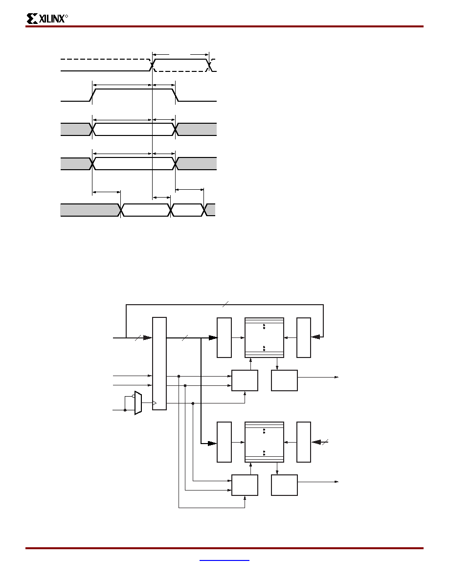
WCLK can be configured as active on either the rising edge
(default) or the falling edge. While the WCLK input to the
RAM accepts the same signal as the clock input to the asso-
ciated CLB’s flip-flops, the sense of this WCLK input can be
inverted with respect to the sense of the flip-flop clock
inputs. Consequently, within the same CLB, data at the
RAMs SPO line can be stored in a flip-flop with either the
same or the inverse clock polarity used to write data to the
RAM.
The WE input is active High and cannot be inverted within
the CLB.
Allowing for settling time, the data on the SPO output
reflects the contents of the RAM location currently
addressed. When the address changes, following the asyn-
chronous delay TILO, the data stored at the new address
location will appear on SPO. If the data at a particular RAM
address is overwritten, after the delay TWOS, the new data
will appear on SPO.
Dual-Port Mode
In dual-port mode, the function generators (F-LUT and
G-LUT) are used to create a 16 x 1 dual-port memory. Of
the two data ports available, one permits read and write
operations at the address specified by A[3:0] while the sec-
ond provides only for read operations at the address speci-
fied independently by DPRA[3:0]. As a result, simultaneous
read/write operations at different addresses (or even at the
same address) are supported.
The functional organization of the 16 x 1 dual-port RAM is
shown in Figure 14. The dual-port RAM signals and the
Figure 13: Data Write and Access Timing for RAM
DS060_13_080400
WCLK (K)
WE
ADDRESS
DATA IN
DATA OUT
OLD
NEW
TDSS
TDHS
TASS
TAHS
TWSS
TWPS
TWHS
TWOS
TILO
Figure 14: Logic Diagram for the Dual-Port RAM
WE
WCLK
A[3:0]
D
4
SPO
DPRA[3:0]
INPUT
REGISTER
WRITE
R
O
W
SELECT
WRITE
CONTROL
READ
OUT
16 x 1
RAM
READ
R
O
W
SELECT
DS060_14_043001
DPO
WRITE
R
O
W
SELECT
WRITE
CONTROL
READ
OUT
16 x 1
RAM
READ
R
O
W
SELECT
相关PDF资料 |
PDF描述 |
|---|---|
| XCS30XL-4TQ84I | Spartan and Spartan-XL Families Field Programmable Gate Arrays |
| XCS30XL-4VQ144C | Spartan and Spartan-XL Families Field Programmable Gate Arrays |
| XCS30XL-4VQ208C | Spartan and Spartan-XL Families Field Programmable Gate Arrays |
| XCS30XL-4VQ208I | Spartan and Spartan-XL Families Field Programmable Gate Arrays |
| XCS30XL-4VQ240C | Spartan and Spartan-XL Families Field Programmable Gate Arrays |
相关代理商/技术参数 |
参数描述 |
|---|---|
| XCS30XL-4TQ84I | 制造商:XILINX 制造商全称:XILINX 功能描述:Spartan and Spartan-XL Families Field Programmable Gate Arrays |
| XCS30XL-4TQG144C | 功能描述:IC SPARTAN-XL FPGA 30K 144-TQFP RoHS:是 类别:集成电路 (IC) >> 嵌入式 - FPGA(现场可编程门阵列) 系列:Spartan®-XL 标准包装:1 系列:Kintex-7 LAB/CLB数:25475 逻辑元件/单元数:326080 RAM 位总计:16404480 输入/输出数:350 门数:- 电源电压:0.97 V ~ 1.03 V 安装类型:表面贴装 工作温度:0°C ~ 85°C 封装/外壳:900-BBGA,FCBGA 供应商设备封装:900-FCBGA(31x31) 其它名称:122-1789 |
| XCS30XL-4TQG144I | 功能描述:IC SPARTAN-XL FPGA 30K 144-TQFP RoHS:是 类别:集成电路 (IC) >> 嵌入式 - FPGA(现场可编程门阵列) 系列:Spartan®-XL 标准包装:1 系列:Kintex-7 LAB/CLB数:25475 逻辑元件/单元数:326080 RAM 位总计:16404480 输入/输出数:350 门数:- 电源电压:0.97 V ~ 1.03 V 安装类型:表面贴装 工作温度:0°C ~ 85°C 封装/外壳:900-BBGA,FCBGA 供应商设备封装:900-FCBGA(31x31) 其它名称:122-1789 |
| XCS30XL-4VQ100C | 功能描述:IC FPGA 3.3V C-TEMP HP 100VQFP RoHS:否 类别:集成电路 (IC) >> 嵌入式 - FPGA(现场可编程门阵列) 系列:Spartan®-XL 标准包装:1 系列:Kintex-7 LAB/CLB数:25475 逻辑元件/单元数:326080 RAM 位总计:16404480 输入/输出数:350 门数:- 电源电压:0.97 V ~ 1.03 V 安装类型:表面贴装 工作温度:0°C ~ 85°C 封装/外壳:900-BBGA,FCBGA 供应商设备封装:900-FCBGA(31x31) 其它名称:122-1789 |
| XCS30XL-4VQ100I | 功能描述:IC FPGA 3.3V I-TEMP HP 100VQFP RoHS:否 类别:集成电路 (IC) >> 嵌入式 - FPGA(现场可编程门阵列) 系列:Spartan®-XL 标准包装:1 系列:Kintex-7 LAB/CLB数:25475 逻辑元件/单元数:326080 RAM 位总计:16404480 输入/输出数:350 门数:- 电源电压:0.97 V ~ 1.03 V 安装类型:表面贴装 工作温度:0°C ~ 85°C 封装/外壳:900-BBGA,FCBGA 供应商设备封装:900-FCBGA(31x31) 其它名称:122-1789 |
发布紧急采购,3分钟左右您将得到回复。