参数资料
| 型号: | XCV400E-7BG560I |
| 厂商: | Xilinx Inc |
| 文件页数: | 152/233页 |
| 文件大小: | 0K |
| 描述: | IC FPGA 1.8V I-TEMP 560-MBGA |
| 产品变化通告: | FPGA Family Discontinuation 18/Apr/2011 |
| 标准包装: | 1 |
| 系列: | Virtex®-E |
| LAB/CLB数: | 2400 |
| 逻辑元件/单元数: | 10800 |
| RAM 位总计: | 163840 |
| 输入/输出数: | 404 |
| 门数: | 569952 |
| 电源电压: | 1.71 V ~ 1.89 V |
| 安装类型: | 表面贴装 |
| 工作温度: | -40°C ~ 100°C |
| 封装/外壳: | 560-LBGA,金属 |
| 供应商设备封装: | 560-MBGA(42.5x42.5) |
第1页第2页第3页第4页第5页第6页第7页第8页第9页第10页第11页第12页第13页第14页第15页第16页第17页第18页第19页第20页第21页第22页第23页第24页第25页第26页第27页第28页第29页第30页第31页第32页第33页第34页第35页第36页第37页第38页第39页第40页第41页第42页第43页第44页第45页第46页第47页第48页第49页第50页第51页第52页第53页第54页第55页第56页第57页第58页第59页第60页第61页第62页第63页第64页第65页第66页第67页第68页第69页第70页第71页第72页第73页第74页第75页第76页第77页第78页第79页第80页第81页第82页第83页第84页第85页第86页第87页第88页第89页第90页第91页第92页第93页第94页第95页第96页第97页第98页第99页第100页第101页第102页第103页第104页第105页第106页第107页第108页第109页第110页第111页第112页第113页第114页第115页第116页第117页第118页第119页第120页第121页第122页第123页第124页第125页第126页第127页第128页第129页第130页第131页第132页第133页第134页第135页第136页第137页第138页第139页第140页第141页第142页第143页第144页第145页第146页第147页第148页第149页第150页第151页当前第152页第153页第154页第155页第156页第157页第158页第159页第160页第161页第162页第163页第164页第165页第166页第167页第168页第169页第170页第171页第172页第173页第174页第175页第176页第177页第178页第179页第180页第181页第182页第183页第184页第185页第186页第187页第188页第189页第190页第191页第192页第193页第194页第195页第196页第197页第198页第199页第200页第201页第202页第203页第204页第205页第206页第207页第208页第209页第210页第211页第212页第213页第214页第215页第216页第217页第218页第219页第220页第221页第222页第223页第224页第225页第226页第227页第228页第229页第230页第231页第232页第233页
Virtex-E 1.8 V Field Programmable Gate Arrays
R
DS022-2 (v3.0) March 21, 2014
Module 2 of 4
Production Product Specification
19
— OBSOLETE — OBSOLETE — OBSOLETE — OBSOLETE —
mits the internal storage elements to begin changing state
in response to the logic and the user clock.
The relative timing of these events can be changed. In addi-
tion, the GTS, GSR, and GWE events can be made depen-
dent on the DONE pins of multiple devices all going High,
forcing the devices to start synchronously. The sequence
can also be paused at any stage until lock has been
achieved on any or all DLLs.
Readback
The configuration data stored in the Virtex-E configuration
memory can be readback for verification. Along with the
configuration data it is possible to readback the contents all
flip-flops/latches, LUT RAMs, and block RAMs. This capa-
bility is used for real-time debugging. For more detailed
information, see application note XAPP138 “Virtex FPGA
Series Configuration and Readback”.
Design Considerations
This section contains more detailed design information on
the following features.
Delay-Locked Loop . . . see page 19
BlockRAM . . . see page 24
SelectI/O . . . see page 31
Using DLLs
The Virtex-E FPGA series provides up to eight fully digital
dedicated on-chip Delay-Locked Loop (DLL) circuits which
provide zero propagation delay, low clock skew between
output clock signals distributed throughout the device, and
advanced clock domain control. These dedicated DLLs can
be used to implement several circuits which improve and
simplify system level design.
Introduction
As FPGAs grow in size, quality on-chip clock distribution
becomes increasingly important. Clock skew and clock
delay impact device performance and the task of managing
clock skew and clock delay with conventional clock trees
becomes more difficult in large devices. The Virtex-E series
of devices resolve this potential problem by providing up to
eight fully digital dedicated on-chip DLL circuits, which pro-
vide zero propagation delay and low clock skew between
output clock signals distributed throughout the device.
Each DLL can drive up to two global clock routing networks
within the device. The global clock distribution network min-
imizes clock skews due to loading differences. By monitor-
ing a sample of the DLL output clock, the DLL can
compensate for the delay on the routing network, effectively
eliminating the delay from the external input port to the indi-
vidual clock loads within the device.
In addition to providing zero delay with respect to a user
source clock, the DLL can provide multiple phases of the
source clock. The DLL can also act as a clock doubler or it
can divide the user source clock by up to 16.
Clock multiplication gives the designer a number of design
alternatives. For instance, a 50 MHz source clock doubled
by the DLL can drive an FPGA design operating at 100
MHz. This technique can simplify board design because the
clock path on the board no longer distributes such a
high-speed signal. A multiplied clock also provides design-
ers the option of time-domain-multiplexing, using one circuit
twice per clock cycle, consuming less area than two copies
of the same circuit. Two DLLs in can be connected in series
to increase the effective clock multiplication factor to four.
The DLL can also act as a clock mirror. By driving the DLL
output off-chip and then back in again, the DLL can be used
to deskew a board level clock between multiple devices.
In order to guarantee the system clock establishes prior to
the device “waking up,” the DLL can delay the completion of
the device configuration process until after the DLL
achieves lock.
By taking advantage of the DLL to remove on-chip clock
delay, the designer can greatly simplify and improve system
level design involving high-fanout, high-performance clocks.
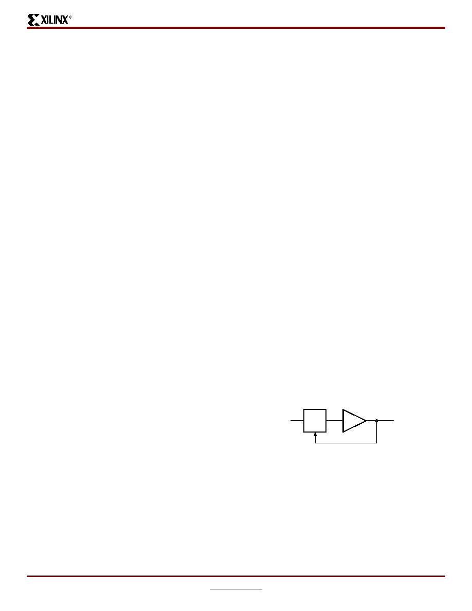
Library DLL Symbols
Figure 21 shows the simplified Xilinx library DLL macro
symbol, BUFGDLL. This macro delivers a quick and effi-
cient way to provide a system clock with zero propagation
the two library DLL primitives. These symbols provide
access to the complete set of DLL features when imple-
menting more complex applications.
Figure 21: Simplified DLL Macro Symbol BUFGDLL
0ns
ds022_25_121099
O
I
相关PDF资料 |
PDF描述 |
|---|---|
| XCV400E-7BG432I | IC FPGA 1.8V I-TEMP 432-MBGA |
| BR93L66RFVM-WTR | IC EEPROM 4KBIT 2MHZ 8MSOP |
| XC2V1500-5BG575I | IC FPGA VIRTEX-II 575PBGA |
| XC2V1500-6BGG575C | IC FPGA VIRTEX-II 1.5M 575-MBGA |
| XC2V1500-5BGG575I | IC FPGA VIRTEX-II 1.5M 575-MBGA |
相关代理商/技术参数 |
参数描述 |
|---|---|
| XCV400E-7FG240C | 制造商:XILINX 制造商全称:XILINX 功能描述:Virtex⑩-E 1.8 V Field Programmable Gate Arrays |
| XCV400E-7FG240I | 制造商:XILINX 制造商全称:XILINX 功能描述:Virtex⑩-E 1.8 V Field Programmable Gate Arrays |
| XCV400E-7FG676C | 功能描述:IC FPGA 1.8V C-TEMP 676-FBGA RoHS:否 类别:集成电路 (IC) >> 嵌入式 - FPGA(现场可编程门阵列) 系列:Virtex®-E 产品变化通告:Step Intro and Pkg Change 11/March/2008 标准包装:1 系列:Virtex®-5 SXT LAB/CLB数:4080 逻辑元件/单元数:52224 RAM 位总计:4866048 输入/输出数:480 门数:- 电源电压:0.95 V ~ 1.05 V 安装类型:表面贴装 工作温度:-40°C ~ 100°C 封装/外壳:1136-BBGA,FCBGA 供应商设备封装:1136-FCBGA 配用:568-5088-ND - BOARD DEMO DAC1408D750122-1796-ND - EVALUATION PLATFORM VIRTEX-5 |
| XCV400E-7FG676I | 功能描述:IC FPGA 1.8V I-TEMP 676-FBGA RoHS:否 类别:集成电路 (IC) >> 嵌入式 - FPGA(现场可编程门阵列) 系列:Virtex®-E 产品变化通告:Step Intro and Pkg Change 11/March/2008 标准包装:1 系列:Virtex®-5 SXT LAB/CLB数:4080 逻辑元件/单元数:52224 RAM 位总计:4866048 输入/输出数:480 门数:- 电源电压:0.95 V ~ 1.05 V 安装类型:表面贴装 工作温度:-40°C ~ 100°C 封装/外壳:1136-BBGA,FCBGA 供应商设备封装:1136-FCBGA 配用:568-5088-ND - BOARD DEMO DAC1408D750122-1796-ND - EVALUATION PLATFORM VIRTEX-5 |
| XCV400E-7HQ240C | 制造商:XILINX 制造商全称:XILINX 功能描述:Virtex-E 1.8 V Field Programmable Gate Arrays |
发布紧急采购,3分钟左右您将得到回复。