参数资料
| 型号: | XCV400E-7BG560I |
| 厂商: | Xilinx Inc |
| 文件页数: | 68/233页 |
| 文件大小: | 0K |
| 描述: | IC FPGA 1.8V I-TEMP 560-MBGA |
| 产品变化通告: | FPGA Family Discontinuation 18/Apr/2011 |
| 标准包装: | 1 |
| 系列: | Virtex®-E |
| LAB/CLB数: | 2400 |
| 逻辑元件/单元数: | 10800 |
| RAM 位总计: | 163840 |
| 输入/输出数: | 404 |
| 门数: | 569952 |
| 电源电压: | 1.71 V ~ 1.89 V |
| 安装类型: | 表面贴装 |
| 工作温度: | -40°C ~ 100°C |
| 封装/外壳: | 560-LBGA,金属 |
| 供应商设备封装: | 560-MBGA(42.5x42.5) |
第1页第2页第3页第4页第5页第6页第7页第8页第9页第10页第11页第12页第13页第14页第15页第16页第17页第18页第19页第20页第21页第22页第23页第24页第25页第26页第27页第28页第29页第30页第31页第32页第33页第34页第35页第36页第37页第38页第39页第40页第41页第42页第43页第44页第45页第46页第47页第48页第49页第50页第51页第52页第53页第54页第55页第56页第57页第58页第59页第60页第61页第62页第63页第64页第65页第66页第67页当前第68页第69页第70页第71页第72页第73页第74页第75页第76页第77页第78页第79页第80页第81页第82页第83页第84页第85页第86页第87页第88页第89页第90页第91页第92页第93页第94页第95页第96页第97页第98页第99页第100页第101页第102页第103页第104页第105页第106页第107页第108页第109页第110页第111页第112页第113页第114页第115页第116页第117页第118页第119页第120页第121页第122页第123页第124页第125页第126页第127页第128页第129页第130页第131页第132页第133页第134页第135页第136页第137页第138页第139页第140页第141页第142页第143页第144页第145页第146页第147页第148页第149页第150页第151页第152页第153页第154页第155页第156页第157页第158页第159页第160页第161页第162页第163页第164页第165页第166页第167页第168页第169页第170页第171页第172页第173页第174页第175页第176页第177页第178页第179页第180页第181页第182页第183页第184页第185页第186页第187页第188页第189页第190页第191页第192页第193页第194页第195页第196页第197页第198页第199页第200页第201页第202页第203页第204页第205页第206页第207页第208页第209页第210页第211页第212页第213页第214页第215页第216页第217页第218页第219页第220页第221页第222页第223页第224页第225页第226页第227页第228页第229页第230页第231页第232页第233页
Virtex-E 1.8 V Field Programmable Gate Arrays
R
Module 2 of 4
DS022-2 (v3.0) March 21, 2014
10
Production Product Specification
— OBSOLETE — OBSOLETE — OBSOLETE — OBSOLETE —
Data Registers
The primary data register is the Boundary Scan register.
For each IOB pin in the FPGA, bonded or not, it includes
three bits for In, Out, and 3-State Control. Non-IOB pins
have appropriate partial bit population if input-only or out-
put-only. Each EXTEST CAPTURED-OR state captures all
In, Out, and 3-state pins.
The other standard data register is the single flip-flop
BYPASS register. It synchronizes data being passed
through the FPGA to the next downstream Boundary Scan
device.
The FPGA supports up to two additional internal scan
chains that can be specified using the BSCAN macro. The
macro provides two user pins (SEL1 and SEL2) which are
decodes of the USER1 and USER2 instructions respec-
tively. For these instructions, two corresponding pins (T
DO1 and TDO2) allow user scan data to be shifted out of
TDO.
Likewise, there are individual clock pins (DRCK1 and
DRCK2) for each user register. There is a common input pin
(TDI) and shared output pins that represent the state of the
TAP controller (RESET, SHIFT, and UPDATE).
Bit Sequence
The order within each IOB is: In, Out, 3-State. The
input-only pins contribute only the In bit to the Boundary
Scan I/O data register, while the output-only pins contrib-
utes all three bits.
From a cavity-up view of the chip (as shown in EPIC), start-
ing in the upper right chip corner, the Boundary Scan
data-register bits are ordered as shown in Figure 12.
BSDL (Boundary Scan Description Language) files for Vir-
tex-E Series devices are available on the Xilinx web site in
the File Download area.
Identification Registers
The IDCODE register is supported. By using the IDCODE,
the device connected to the JTAG port can be determined.
The IDCODE register has the following binary format:
vvvv:ffff:fffa:aaaa:aaaa:cccc:cccc:ccc1
where
v = the die version number
f = the family code (05 for Virtex-E family)
a = the number of CLB rows (ranges from 16 for
XCV50E to 104 for XCV3200E)
c = the company code (49h for Xilinx)
The USERCODE register is supported. By using the USER-
CODE, a user-programmable identification code can be
loaded and shifted out for examination. The identification
code (see Table 7) is embedded in the bitstream during bit-
stream generation and is valid only after configuration.
Note:
Attempting to load an incorrect bitstream causes
configuration to fail and can damage the device.
Including Boundary Scan in a Design
Since the Boundary Scan pins are dedicated, no special
element needs to be added to the design unless an internal
data register (USER1 or USER2) is desired.
If an internal data register is used, insert the Boundary Scan
symbol and connect the necessary pins as appropriate.
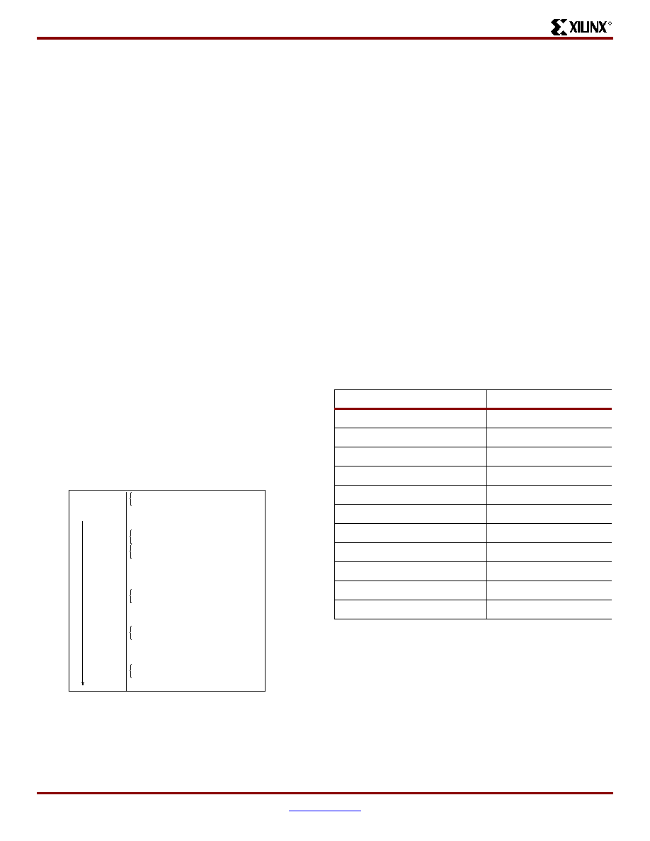
Figure 12: Boundary Scan Bit Sequence
Bit 0 ( TDO end)
Bit 1
Bit 2
Right half of top-edge IOBs (Right to Left)
GCLK2
GCLK3
Left half of top-edge IOBs (Right to Left)
Left-edge IOBs (Top to Bottom)
M1
M0
M2
Left half of bottom-edge IOBs (Left to Right)
GCLK1
GCLK0
Right half of bottom-edge IOBs (Left to Right)
DONE
PROG
Right-edge IOBs (Bottom to Top)
CCLK
(TDI end)
990602001
Table 7: IDCODEs Assigned to Virtex-E FPGAs
FPGA
IDCODE
XCV50E
v0A10093h
XCV100E
v0A14093h
XCV200E
v0A1C093h
XCV300E
v0A20093h
XCV400E
v0A28093h
XCV600E
v0A30093h
XCV1000E
v0A40093h
XCV1600E
v0A48093h
XCV2000E
v0A50093h
XCV2600E
v0A5C093h
XCV3200E
v0A68093h
相关PDF资料 |
PDF描述 |
|---|---|
| XCV400E-7BG432I | IC FPGA 1.8V I-TEMP 432-MBGA |
| BR93L66RFVM-WTR | IC EEPROM 4KBIT 2MHZ 8MSOP |
| XC2V1500-5BG575I | IC FPGA VIRTEX-II 575PBGA |
| XC2V1500-6BGG575C | IC FPGA VIRTEX-II 1.5M 575-MBGA |
| XC2V1500-5BGG575I | IC FPGA VIRTEX-II 1.5M 575-MBGA |
相关代理商/技术参数 |
参数描述 |
|---|---|
| XCV400E-7FG240C | 制造商:XILINX 制造商全称:XILINX 功能描述:Virtex⑩-E 1.8 V Field Programmable Gate Arrays |
| XCV400E-7FG240I | 制造商:XILINX 制造商全称:XILINX 功能描述:Virtex⑩-E 1.8 V Field Programmable Gate Arrays |
| XCV400E-7FG676C | 功能描述:IC FPGA 1.8V C-TEMP 676-FBGA RoHS:否 类别:集成电路 (IC) >> 嵌入式 - FPGA(现场可编程门阵列) 系列:Virtex®-E 产品变化通告:Step Intro and Pkg Change 11/March/2008 标准包装:1 系列:Virtex®-5 SXT LAB/CLB数:4080 逻辑元件/单元数:52224 RAM 位总计:4866048 输入/输出数:480 门数:- 电源电压:0.95 V ~ 1.05 V 安装类型:表面贴装 工作温度:-40°C ~ 100°C 封装/外壳:1136-BBGA,FCBGA 供应商设备封装:1136-FCBGA 配用:568-5088-ND - BOARD DEMO DAC1408D750122-1796-ND - EVALUATION PLATFORM VIRTEX-5 |
| XCV400E-7FG676I | 功能描述:IC FPGA 1.8V I-TEMP 676-FBGA RoHS:否 类别:集成电路 (IC) >> 嵌入式 - FPGA(现场可编程门阵列) 系列:Virtex®-E 产品变化通告:Step Intro and Pkg Change 11/March/2008 标准包装:1 系列:Virtex®-5 SXT LAB/CLB数:4080 逻辑元件/单元数:52224 RAM 位总计:4866048 输入/输出数:480 门数:- 电源电压:0.95 V ~ 1.05 V 安装类型:表面贴装 工作温度:-40°C ~ 100°C 封装/外壳:1136-BBGA,FCBGA 供应商设备封装:1136-FCBGA 配用:568-5088-ND - BOARD DEMO DAC1408D750122-1796-ND - EVALUATION PLATFORM VIRTEX-5 |
| XCV400E-7HQ240C | 制造商:XILINX 制造商全称:XILINX 功能描述:Virtex-E 1.8 V Field Programmable Gate Arrays |
发布紧急采购,3分钟左右您将得到回复。