参数资料
| 型号: | XCV400E-7BG560I |
| 厂商: | Xilinx Inc |
| 文件页数: | 35/233页 |
| 文件大小: | 0K |
| 描述: | IC FPGA 1.8V I-TEMP 560-MBGA |
| 产品变化通告: | FPGA Family Discontinuation 18/Apr/2011 |
| 标准包装: | 1 |
| 系列: | Virtex®-E |
| LAB/CLB数: | 2400 |
| 逻辑元件/单元数: | 10800 |
| RAM 位总计: | 163840 |
| 输入/输出数: | 404 |
| 门数: | 569952 |
| 电源电压: | 1.71 V ~ 1.89 V |
| 安装类型: | 表面贴装 |
| 工作温度: | -40°C ~ 100°C |
| 封装/外壳: | 560-LBGA,金属 |
| 供应商设备封装: | 560-MBGA(42.5x42.5) |
第1页第2页第3页第4页第5页第6页第7页第8页第9页第10页第11页第12页第13页第14页第15页第16页第17页第18页第19页第20页第21页第22页第23页第24页第25页第26页第27页第28页第29页第30页第31页第32页第33页第34页当前第35页第36页第37页第38页第39页第40页第41页第42页第43页第44页第45页第46页第47页第48页第49页第50页第51页第52页第53页第54页第55页第56页第57页第58页第59页第60页第61页第62页第63页第64页第65页第66页第67页第68页第69页第70页第71页第72页第73页第74页第75页第76页第77页第78页第79页第80页第81页第82页第83页第84页第85页第86页第87页第88页第89页第90页第91页第92页第93页第94页第95页第96页第97页第98页第99页第100页第101页第102页第103页第104页第105页第106页第107页第108页第109页第110页第111页第112页第113页第114页第115页第116页第117页第118页第119页第120页第121页第122页第123页第124页第125页第126页第127页第128页第129页第130页第131页第132页第133页第134页第135页第136页第137页第138页第139页第140页第141页第142页第143页第144页第145页第146页第147页第148页第149页第150页第151页第152页第153页第154页第155页第156页第157页第158页第159页第160页第161页第162页第163页第164页第165页第166页第167页第168页第169页第170页第171页第172页第173页第174页第175页第176页第177页第178页第179页第180页第181页第182页第183页第184页第185页第186页第187页第188页第189页第190页第191页第192页第193页第194页第195页第196页第197页第198页第199页第200页第201页第202页第203页第204页第205页第206页第207页第208页第209页第210页第211页第212页第213页第214页第215页第216页第217页第218页第219页第220页第221页第222页第223页第224页第225页第226页第227页第228页第229页第230页第231页第232页第233页
Virtex-E 1.8 V Field Programmable Gate Arrays
R
DS022-2 (v3.0) March 21, 2014
Module 2 of 4
Production Product Specification
7
— OBSOLETE — OBSOLETE — OBSOLETE — OBSOLETE —
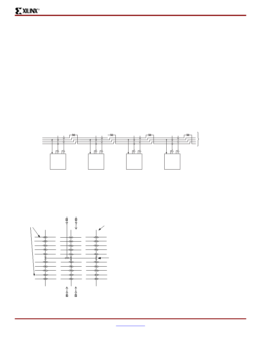
Dedicated Routing
Some classes of signal require dedicated routing resources to
maximize performance. In the Virtex-E architecture, dedi-
cated routing resources are provided for two classes of signal.
Horizontal routing resources are provided for on-chip
3-state buses. Four partitionable bus lines are provided
per CLB row, permitting multiple buses within a row, as
shown in Figure 8.
Two dedicated nets per CLB propagate carry signals
vertically to the adjacent CLB.Global Clock Distribution
Network
DLL Location
Clock Routing
Clock Routing resources distribute clocks and other signals
with very high fanout throughout the device. Virtex-E
devices include two tiers of clock routing resources referred
to as global and local clock routing resources.
The global routing resources are four dedicated global
nets with dedicated input pins that are designed to
distribute high-fanout clock signals with minimal skew.
Each global clock net can drive all CLB, IOB, and block
RAM clock pins. The global nets can be driven only by
global buffers. There are four global buffers, one for
each global net.
The local clock routing resources consist of 24
backbone lines, 12 across the top of the chip and 12
across bottom. From these lines, up to 12 unique
signals per column can be distributed via the 12
longlines in the column. These local resources are
more flexible than the global resources since they are
not restricted to routing only to clock pins.
Global Clock Distribution
Virtex-E provides high-speed, low-skew clock distribution
through the global routing resources described above. A
typical clock distribution net is shown in Figure 9.
Four global buffers are provided, two at the top center of the
device and two at the bottom center. These drive the four
global nets that in turn drive any clock pin.
Four dedicated clock pads are provided, one adjacent to
each of the global buffers. The input to the global buffer is
selected either from these pads or from signals in the gen-
eral purpose routing.
Digital Delay-Locked Loops
There are eight DLLs (Delay-Locked Loops) per device,
with four located at the top and four at the bottom,
Figure 10. The DLLs can be used to eliminate skew
between the clock input pad and the internal clock input pins
throughout the device. Each DLL can drive two global clock
networks.The DLL monitors the input clock and the distrib-
uted clock, and automatically adjusts a clock delay element.
Additional delay is introduced such that clock edges arrive
at internal flip-flops synchronized with clock edges arriving
at the input.
In addition to eliminating clock-distribution delay, the DLL
provides advanced control of multiple clock domains. The
DLL provides four quadrature phases of the source clock,
and can double the clock or divide the clock by 1.5, 2, 2.5, 3,
4, 5, 8, or 16.
Figure 8: BUFT Connections to Dedicated Horizontal Bus LInes
CLB
buft_c.eps
Tri-State
Lines
Figure 9: Global Clock Distribution Network
Gl
ob
al
Clo
c
k
Sp
in
e
Global Clock Column
GCLKPAD2
GCLKBUF2
GCLKPAD3
GCLKBUF3
GCLKBUF1
GCLKPAD1
GCLKBUF0
GCLKPAD0
Global Clock Rows
XCVE_009
相关PDF资料 |
PDF描述 |
|---|---|
| XCV400E-7BG432I | IC FPGA 1.8V I-TEMP 432-MBGA |
| BR93L66RFVM-WTR | IC EEPROM 4KBIT 2MHZ 8MSOP |
| XC2V1500-5BG575I | IC FPGA VIRTEX-II 575PBGA |
| XC2V1500-6BGG575C | IC FPGA VIRTEX-II 1.5M 575-MBGA |
| XC2V1500-5BGG575I | IC FPGA VIRTEX-II 1.5M 575-MBGA |
相关代理商/技术参数 |
参数描述 |
|---|---|
| XCV400E-7FG240C | 制造商:XILINX 制造商全称:XILINX 功能描述:Virtex⑩-E 1.8 V Field Programmable Gate Arrays |
| XCV400E-7FG240I | 制造商:XILINX 制造商全称:XILINX 功能描述:Virtex⑩-E 1.8 V Field Programmable Gate Arrays |
| XCV400E-7FG676C | 功能描述:IC FPGA 1.8V C-TEMP 676-FBGA RoHS:否 类别:集成电路 (IC) >> 嵌入式 - FPGA(现场可编程门阵列) 系列:Virtex®-E 产品变化通告:Step Intro and Pkg Change 11/March/2008 标准包装:1 系列:Virtex®-5 SXT LAB/CLB数:4080 逻辑元件/单元数:52224 RAM 位总计:4866048 输入/输出数:480 门数:- 电源电压:0.95 V ~ 1.05 V 安装类型:表面贴装 工作温度:-40°C ~ 100°C 封装/外壳:1136-BBGA,FCBGA 供应商设备封装:1136-FCBGA 配用:568-5088-ND - BOARD DEMO DAC1408D750122-1796-ND - EVALUATION PLATFORM VIRTEX-5 |
| XCV400E-7FG676I | 功能描述:IC FPGA 1.8V I-TEMP 676-FBGA RoHS:否 类别:集成电路 (IC) >> 嵌入式 - FPGA(现场可编程门阵列) 系列:Virtex®-E 产品变化通告:Step Intro and Pkg Change 11/March/2008 标准包装:1 系列:Virtex®-5 SXT LAB/CLB数:4080 逻辑元件/单元数:52224 RAM 位总计:4866048 输入/输出数:480 门数:- 电源电压:0.95 V ~ 1.05 V 安装类型:表面贴装 工作温度:-40°C ~ 100°C 封装/外壳:1136-BBGA,FCBGA 供应商设备封装:1136-FCBGA 配用:568-5088-ND - BOARD DEMO DAC1408D750122-1796-ND - EVALUATION PLATFORM VIRTEX-5 |
| XCV400E-7HQ240C | 制造商:XILINX 制造商全称:XILINX 功能描述:Virtex-E 1.8 V Field Programmable Gate Arrays |
发布紧急采购,3分钟左右您将得到回复。