参数资料
| 型号: | XOCLCC6EVB |
| 厂商: | ON Semiconductor |
| 文件页数: | 3/9页 |
| 文件大小: | 0K |
| 描述: | EVAL BOARD FOR XOCLCC6 |
| 设计资源: | XOCLCC6EVB Gerber Files |
| 标准包装: | 1 |
| 主要目的: | 计时,时钟振荡器 |
| 嵌入式: | 否 |
| 已用 IC / 零件: | NBXxxxx 时钟振荡器,6-CLCC 封装 |
| 主要属性: | 用于 6-CLCC NBXxxxx 振荡器的衬垫 |
| 次要属性: | 单电源或分离式电源 |
| 已供物品: | 板 |
| 其它名称: | XOCLCC6EVBOS |
�� �
�
�XOCLCC6EVB�
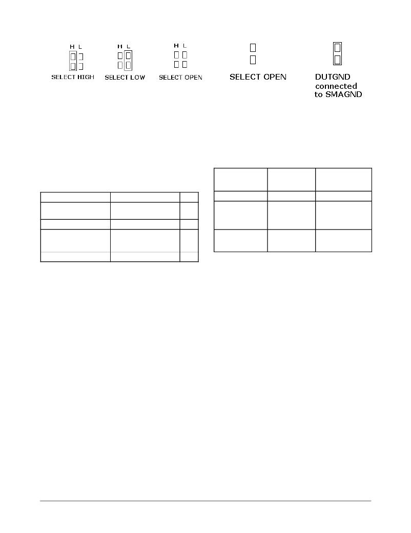
�Evaluation� Board� Jumper� Headers� on� OE� (Pin� 4),� FSEL� (Pin� 5)�
�Evaluation� Board� Jumper� Header� on� DUTGND� (Pin� 3)�
�Figure� 3.� Select� Positions� for� Evaluation� Board� Jumper� Headers� on� OE� (Pin� 4),� FSEL� (Pin� 5),� and� DUTGND� (Pin� 3)�
�TIME� DOMAIN� MEASUREMENTS�
�Equipment�
�Table� 2� indicates� the� recommended� equipment� for�
�making� characterization� and� performance� measurements.�
�Table� 2.� BASIC� EQUIPMENT�
�Table� 3.� XOCLCC6EVB� POWER� SUPPLY�
�CONNECTION� VOLTAGES�
�A).� Single� C).� Single�
�Positive� B).� Split� 3.3� V� Negative�
�+3.3� V� Setup� Setup� ?� 3.3� V� Setup�
�Description�
�Power� Supply� with� 4�
�outputs�
�Real� ?� Time� Oscilloscope�
�Matched� High� Speed�
�Cables� with� SMA�
�Connectors�
�Example� Equipment�
�HP6624A� or� similar�
�DPO70804� or� similar�
�Storm,� Semflex,� or�
�similar�
�Qty�
�1�
�1�
�2�
�V� DD� =� 3.3� V�
�V� TT�
�=� V� DD� ?� 2.0� V�
�=� 1.3� V�
�DUTGND�
�=� SMAGND�
�=0V�
�V� DD� =� 2.0� V�
�V� TT�
�=� V� DD� ?� 2.0� V�
�=� SMAGND�
�=0V�
�DUTGND�
�=� ?� 1.3� V�
�V� DD� =� 0� V�
�V� TT�
�=� V� DD� ?� 2.0� V�
�=� ?� 2.0� V� SMAGND�
�=� V� DD� =� 0� V�
�DUTGND� =� ?� 3.3� V�
�Power� supply� cables�
�4�
�NOTE:� SMAGND� is� the� SMA� cable� shield� reference� for�
�Setup�
�The� following� steps� should� be� followed� for� proper�
�equipment� setup.�
�Step� 1:� Connect� Power� (split� power� supply� mode)�
�Three� power� levels� must� be� provided� to� the� board:� V� DD� ,�
�DUTGND,� and� SMAGND� via� the� test� point� anvils� at� the�
�edges� of� the� board.� Bypass� capacitors� are� installed� from�
�V� DD� to� SMAGND� and� DUTGND� to� SMAGND� near� the� test�
�points� (see� BOM).� Devices� may� be� tested� in� one� of� three�
�supply� modes� (see� Table� 3):�
�A).� Single� (Positive)� +3.3� V� Setup�
�No� offset� to� supplies� or� output� levels�
�B).� Split� 3.3� V� Setup�
�Offsets� the� V� DD� ,� DUTGND,� and� output� voltage� levels� by�
�?� 1.3� V� and� avoids� an� additional,� separate� V� TT� supply� and�
�allows� a� direct� connection� to� test� equipment� such� as� an�
�oscilloscope� or� counter� with� 50� W� impedance� to� GND�
�inputs.� SMAGND� =� V� TT� =� V� DD� –� 2.0� V� =� 0.0� V.�
�C).� Single� (Negative)� ?� 3.3� V� Setup�
�Offsets� the� V� DD� ,� DUTGND,� and� output� voltage� levels� by�
�?� 3.3� V�
�the� inputs� and� outputs� only,� not� to� be� confused�
�with� the� device� ground� pin� (DUTGND).�
�Step� 2:� Connect� Output� Signals�
�Table� 4� gives� a� list� of� specific� LOGIC� Levels� and� their�
�appropriate� Power� Supply� and� Typical� Lab� Setup�
�conditions�
�LVPECL� :� The� LVPECL� outputs� have� standard,� open�
�emitter� outputs� and� must� be� externally� DC� loaded� and� AC�
�terminated.� A� split� power� supply� technique� takes� advantage�
�of� terminating� the� LVPECL� outputs� into� 50� W� of� an�
�oscilloscope� or� a� frequency� counter.� Since� V� TT� =� V� DD� –� 2� V,�
�offsetting� V� DD� to� +2.0� V� yields� V� TT� =� 0� V� or� Ground�
�(SMAGND).� The� V� TT� terminal� connects� to� the� isolated�
�SMAGND� connector� ground� plane,� and� is� not� to� be�
�confused� with� the� device� ground� pin� (DUTGND).� (See�
�Application� Note� AN8020/D� for� details� on� ECL�
�termination).�
�CML� :� For� CML� lab� setup� and� test,� operation� with�
�negative� supply� voltage� is� recommended� to� enable� the� 50� W�
�internal� impedance� in� the� oscilloscope� to� be� used� as� a�
�termination� of� the� CML� signals� (V� DD� =� 0.0� V,� SMAGND� =�
�0.0� V,� and� DUTGND� =� ?� 3.3� V� (See� Application� Note�
�AN8173/D� for� details� on� CML� termination).�
�http://onsemi.com�
�3�
�相关PDF资料 |
PDF描述 |
|---|---|
| XR16M890IL32-0C-EB | BOARD EVAL XR16M890IL32 |
| XR18W750/753-0B-EB | EVAL BOARD FOR XR18W750/753 |
| XRP2526EVB | BOARD EVAL POWER SWITCH XRP2526 |
| XRP2528EVB | BOARD EVAL POWER SWITCH XRP2528 |
| XT800SM | GAS TRIGGER TUBE 800V SMD |
相关代理商/技术参数 |
参数描述 |
|---|---|
| XOCSM101 | 制造商:RFM 制造商全称:RF Monolithics, Inc 功能描述:10.000000 MHz OCXO |
| XOCSM102 | 制造商:RFM 制造商全称:RF Monolithics, Inc 功能描述:10.000000 MHz OCXO |
| XOCSM103 | 制造商:RFM 制造商全称:RF Monolithics, Inc 功能描述:10.000000 MHz OCXO |
| XOD17 - 36B | 制造商:IXYS Corporation 功能描述:SOLAR DIE 0.63V 126MA |
| XOD17 - 04B | 制造商:IXYS Corporation 功能描述:SOLAR DIE 0.63V 12MA |
发布紧急采购,3分钟左右您将得到回复。