- 您现在的位置:买卖IC网 > PDF目录11833 > XR16C850CJ-F (Exar Corporation)IC UART FIFO 128B 44PLCC PDF资料下载
参数资料
| 型号: | XR16C850CJ-F |
| 厂商: | Exar Corporation |
| 文件页数: | 34/56页 |
| 文件大小: | 0K |
| 描述: | IC UART FIFO 128B 44PLCC |
| 标准包装: | 27 |
| 特点: | * |
| 通道数: | 1,UART |
| FIFO's: | 128 字节 |
| 规程: | RS485 |
| 电源电压: | 2.97 V ~ 5.5 V |
| 带自动流量控制功能: | 是 |
| 带IrDA 编码器/解码器: | 是 |
| 带故障启动位检测功能: | 是 |
| 带调制解调器控制功能: | 是 |
| 带CMOS: | 是 |
| 安装类型: | 表面贴装 |
| 封装/外壳: | 44-LCC(J 形引线) |
| 供应商设备封装: | 44-PLCC(16.59x16.59) |
| 包装: | 管件 |
第1页第2页第3页第4页第5页第6页第7页第8页第9页第10页第11页第12页第13页第14页第15页第16页第17页第18页第19页第20页第21页第22页第23页第24页第25页第26页第27页第28页第29页第30页第31页第32页第33页当前第34页第35页第36页第37页第38页第39页第40页第41页第42页第43页第44页第45页第46页第47页第48页第49页第50页第51页第52页第53页第54页第55页第56页
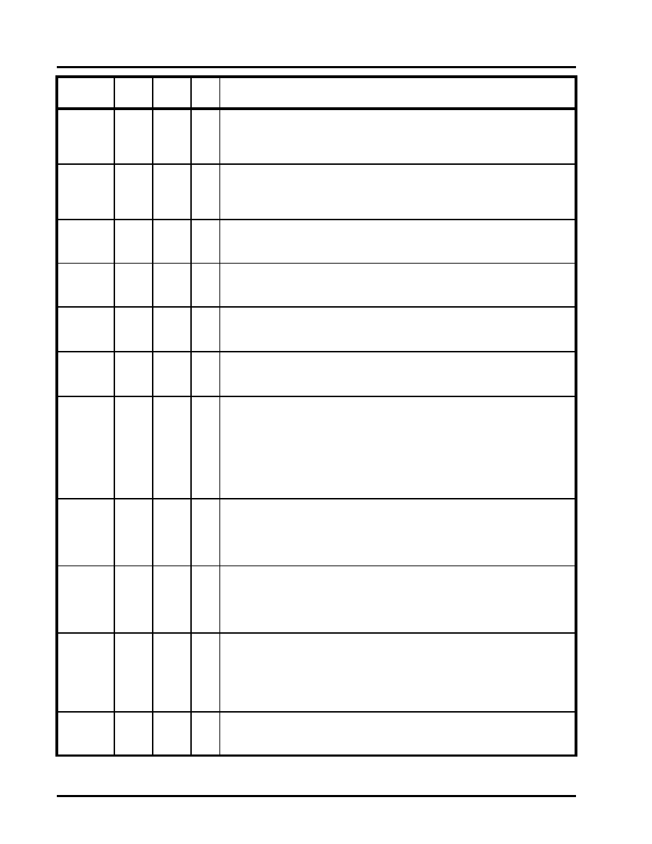
XR16C850
xr
2.97V TO 5.5V UART WITH 128-BYTE FIFO
REV. 2.3.1
4
CS0
14
9
I
Chip Select 0 input (active high). This input selects the XR16C850 device. If CS1 or
CS2# is used as the chip select then this pin must be connected to VCC. During
PC Mode, this pin becomes A5. Caution: SEE”FACTORY TEST MODE” ON
CS1
15
10
I
Chip Select 1 input (active high). This input selects the XR16C850 device. If CS0 or
CS2# is used as the chip select then this pin must be connected to VCC. During
PC Mode, this pin becomes A6. Caution: SEE”FACTORY TEST MODE” ON
CS2#
16
11
I
Chip Select 2 input (active low). This input selects the XR16C850 device. If CS0 or
CS1 is used as the chip select then this pin must be connected to GND. During PC
Mode, this pin becomes A7. Caution: SEE”FACTORY TEST MODE” ON PAGE 7.
INT
33
30
O
Interrupt Output. This output becomes active whenever the transmitter, receiver,
line and/or modem status register has an active condition and is enabled by IER.
See interrupt section for more details. During PC mode, this pin becomes IRQA.
RXRDY#
32
29
O
Receive Ready (active low). A logic 0 indicates receive data ready status, i.e. the
RHR is full or the FIFO has one or more RX characters available for unloading. For
details, see
Table 2. During PC Mode, this pin becomes IRQB.
TXRDY#
27
23
O
Transmit Ready (active low). Buffer ready status is indicated by a logic 0, i.e. at
least one location is empty and available in the FIFO or THR. For details, see
Table 2. During PC Mode, this pin becomes IRQC.
AS#
28
24
I
Address Strobe input (active low). In the Intel bus mode, the leading-edge transition
of AS# latches the chip selects (CS0, CS1, CS2#) and the address lines A0, A1
and A2. This input is used when the address lines are not stable for the duration of
a read or write operation. In devices with top mark date code of "F2 YYWW" and
newer, the address bus is latched even if this input is not used. These devices fea-
ture a ’0 ns’ address hold time. See “AC Electrical Characteristics” . If not required,
this input can be permanently tied to GND. During PC Mode, this pin becomes
AEN#.
D10
D11
D12
-
48
1
22
O
High order data bus. When BUS8/16 is selected as 16 bit data bus mode (BUS8/16
is grounded), RX data errors (break, parity, framing) can be read via these pins.
D10 = Parity, D11 = Framing, and D12 = Break. When BUS8/16 is selected as 8 bit
data bus mode (BUS8/16 is at VCC), D10 and D11 are inactive and D12 becomes
DDIS#. During PC Mode, D10 and D11 are inactive and D12 becomes LPT2#.
BUS8/16
-
25
I
8 or 16 Bit Bus select. For normal 8 bit operation, this pin should be connected to
VCC or left open. To select 16 bit bus mode, this pin should be connected to GND.
When 16 bit bus mode is enabled, DDIS# becomes D12. 16 bit bus mode is not
available for PC Mode. Only RX data error will be provided during this operation.
This pin has an internal pull-up resistor.
CLKSEL
-
13
I
Clock Select. The div-by-1 or div-by-4 pre-scaleable clock is selected by this pin.
The div-by-1 clock is selected when CLKSEL is connected to VCC or the div-by-4
is selected when CLKSEL is connected to GND. MCR bit-7 can override the state
of this pin following reset or initialization (see MCR bit-7). This pin is not available
on 40 and 44 pin packages which provide MCR bit-7 selection only. This pin has
an internal pull-up resistor.
RCLK
10
5
I
This input is used as external 16X clock input to the receiver section. If not used,
connect the -BAUDOUT pin to this input externally. During PC Mode, this pin
becomes S2.
NAME
44-PIN
PLCC
48-PIN
TQFP
TYPE
DESCRIPTION
相关PDF资料 |
PDF描述 |
|---|---|
| MS3116F16-23P | CONN PLUG 23POS STRAIGHT W/PINS |
| XR16C2852CJTR-F | IC UART FIFO 128B 44PLCC |
| D38999/20FB5SA | CONN RCPT 5POS WALL MNT W/SCKT |
| XR16C2850CJTR-F | IC UART FIFO 128B 44PLCC |
| XR68C192IJ-F | IC UART FIFI DUAL 44PLCC |
相关代理商/技术参数 |
参数描述 |
|---|---|
| XR16C850CJTR-F | 制造商:Exar Corporation 功能描述:UART 1-CH 128Byte FIFO 3.3V/5V 44-Pin PLCC T/R 制造商:Exar Corporation 功能描述:XR16C850CJTR-F |
| XR16C850CM | 制造商:Rochester Electronics LLC 功能描述: 制造商:Exar Corporation 功能描述: |
| XR16C850CM-0A-EVB | 功能描述:UART 接口集成电路 Supports C850 48 ld TQFP, ISA Interface RoHS:否 制造商:Texas Instruments 通道数量:2 数据速率:3 Mbps 电源电压-最大:3.6 V 电源电压-最小:2.7 V 电源电流:20 mA 最大工作温度:+ 85 C 最小工作温度:- 40 C 封装 / 箱体:LQFP-48 封装:Reel |
| XR16C850CM-F | 功能描述:UART 接口集成电路 UARTW/128BYTE FIFO RoHS:否 制造商:Texas Instruments 通道数量:2 数据速率:3 Mbps 电源电压-最大:3.6 V 电源电压-最小:2.7 V 电源电流:20 mA 最大工作温度:+ 85 C 最小工作温度:- 40 C 封装 / 箱体:LQFP-48 封装:Reel |
| XR16C850CMTR-F | 功能描述:UART 接口集成电路 UART w/128 Bytes FIFO & IrDA RoHS:否 制造商:Texas Instruments 通道数量:2 数据速率:3 Mbps 电源电压-最大:3.6 V 电源电压-最小:2.7 V 电源电流:20 mA 最大工作温度:+ 85 C 最小工作温度:- 40 C 封装 / 箱体:LQFP-48 封装:Reel |
发布紧急采购,3分钟左右您将得到回复。