- 您现在的位置:买卖IC网 > PDF目录16986 > XRD98L63ZEVAL (Exar Corporation)EVAL BOARD FOR XRD98L63 PDF资料下载
参数资料
| 型号: | XRD98L63ZEVAL |
| 厂商: | Exar Corporation |
| 文件页数: | 10/41页 |
| 文件大小: | 0K |
| 描述: | EVAL BOARD FOR XRD98L63 |
| 标准包装: | 1 |
| 系列: | * |
第1页第2页第3页第4页第5页第6页第7页第8页第9页当前第10页第11页第12页第13页第14页第15页第16页第17页第18页第19页第20页第21页第22页第23页第24页第25页第26页第27页第28页第29页第30页第31页第32页第33页第34页第35页第36页第37页第38页第39页第40页第41页
XRD98L63
18
Rev.1.01
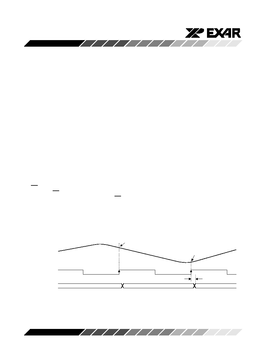
Figure 9. Direct ADC Input Mode Timing
ANALOG TO DIGITAL CONVERTER (ADC)
The analog-to-digital converter is based on pipeline
architecture with a built in track & hold input stage. The
track & hold and ADC conversion are controlled by the
externally supplied ADCLK.
The polarity of the ADCLK is programmable. If
ADCpol=low, the track & hold circuit tracks the PGA
output while ADCLK is high and holds while ADCLK is
low. If ADCpol=high, the track & hold circuit tracks the
PGA output while ADCLK is low and holds while ADCLK
is high. ADCLK should be a 50% duty cycle clock, and
should be synchronized with SBLK such that ADC
tracking ends at the same time as the CDS sample
black ends. (See Figure 16).
The ADC reference levels, Vcm, CapP & CapN, are
generated from an internal voltage reference. To mini-
mize noise, these pins should have high frequency
bypass capacitors to AGND. The value of these ca-
pacitors will affect the time required for the reference to
charge up and settle after power-down mode.
The ADC output bus, DB[11:0], has 3-state capability
controlled by the OE bit of the Control register and pin
42, OE. The output bus is enabled when both the OE bit
is high and the OE pin is low. The outputs become high
impedance when either the OE bit is low or the OE pin
is high.
Direct ADC Input Mode
The Direct ADC Input mode connects the CCDin &
REFin pins directly to the ADC inputs, by-passing the
CDS & PGA circuits. To enable the Direct ADC Input
mode, use the Serial Interface to program:
ADCin=1 in the Test register,
DOclamp=0 in the Clock register, and
MinClip=0 in the Control register.
In this mode, the PGA outputs are disabled so there is
no contention at the ADC input nodes. For best perfor-
mance, we recommend using fully differential signals
with a common mode level around 1.2V.
Input Signal
REFin-CCDin
ADCLK
Sample N
ADC tracks
Input Signal
DB[11:0]
Sample N+1
Data N-6
Data N-5
t
DL
Data N-7
相关PDF资料 |
PDF描述 |
|---|---|
| RCB13DHLN | CONN EDGECARD 26POS DIP .050 SLD |
| P1330R-104K | INDUCTOR POWER 100.0UH SMD |
| VI-270-EY | CONVERTER MOD DC/DC 5V 50W |
| 0210490388 | CABLE JUMPER 1.25MM .030M 32POS |
| VE-20X-EY | CONVERTER MOD DC/DC 5.2V 50W |
相关代理商/技术参数 |
参数描述 |
|---|---|
| XRDAN27 | 制造商:EXAR 制造商全称:EXAR 功能描述:Compensating for Zero Order Hold Effects |
| XRDAN28 | 制造商:EXAR 制造商全称:EXAR 功能描述:Frequency Response Effects of Overampling and Averaging on A/D Output Data |
| XRDAN29 | 制造商:EXAR 制造商全称:EXAR 功能描述:Criteria for Accurate Sampling of Analog Signals |
| XRDAN30 | 制造商:EXAR 制造商全称:EXAR 功能描述:CMOS Current Output D/A Converter Design Concepts for Wide Bandwidth Applications |
| XR-E | 制造商:CREE 制造商全称:Cree, Inc 功能描述:XLamp XR-E and XR-C LED Binning and Labeling |
发布紧急采购,3分钟左右您将得到回复。