- 您现在的位置:买卖IC网 > PDF目录16986 > XRD98L63ZEVAL (Exar Corporation)EVAL BOARD FOR XRD98L63 PDF资料下载
参数资料
| 型号: | XRD98L63ZEVAL |
| 厂商: | Exar Corporation |
| 文件页数: | 6/41页 |
| 文件大小: | 0K |
| 描述: | EVAL BOARD FOR XRD98L63 |
| 标准包装: | 1 |
| 系列: | * |
第1页第2页第3页第4页第5页当前第6页第7页第8页第9页第10页第11页第12页第13页第14页第15页第16页第17页第18页第19页第20页第21页第22页第23页第24页第25页第26页第27页第28页第29页第30页第31页第32页第33页第34页第35页第36页第37页第38页第39页第40页第41页
XRD98L63
14
Rev.1.01
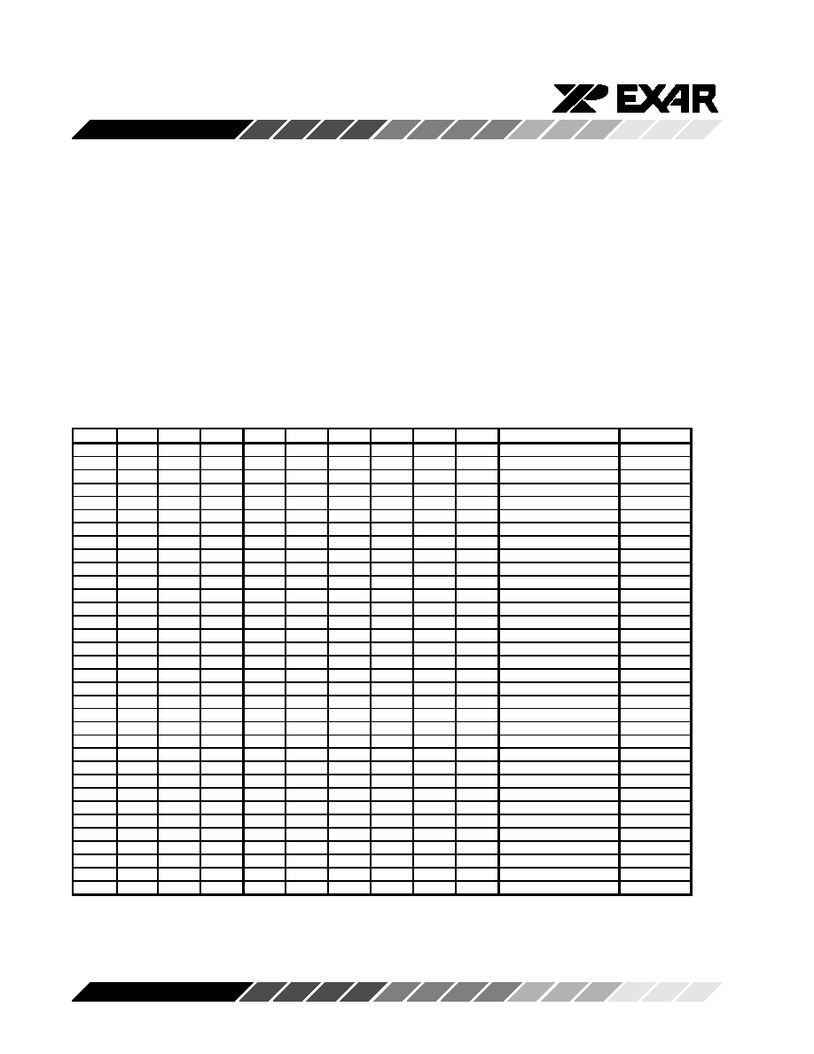
Serial Interface Readback
The readback function is used to view the content of
the serial interface registers as well as several key
registers in the ofset calibration logic. Readback is
enabled by writing a 1 to the RBenable bit (D9) of the
Readback register.
In the readback mode, the content of the selected
register is output on the 10 MSBs of the ADC output
bus pins DB[11:2]. As long as valid clocks and CCD
signal are applied, the calibration will continue to
function properly during readback (internally the ADC
data is still sent to the calibration logic).
Registers are selected for readback by writing to the
RBreg[8:0] bits in the Readback register, bits D8 to D0.
If RBreg[8:6]=000, then RBreg[5:0] are used to ad-
dress the serial interface registers. Currently only
register addresses 0 to 23, 62 and 63 are defined. If
RBreg[8:6]
≠000, then RBreg[5:0] are ignored and
RBreg[8:6] are used to address registers in the calibra-
tion logic.
RBenable RBreg[8] RBreg[7] RBreg[6] RBreg[5] RBreg[4] RBreg[3] RBreg[2] RBreg[1] RBreg[0]
Selected Register
Register Number
0
x
none (ADC data output)
1
0
PGA00
0
1
0
1
Offset
1
0
1
0
PGA01
2
1
0
1
PGA10
3
1
0
1
0
PGA11
4
1
0
1
0
1
OB Even Gain
5
1
0
1
0
OB Odd Gain
6
1
0
1
Even Line
7
1
0
1
0
Odd Line
8
1
0
1
0
1
Calibration
9
1
0
1
0
1
0
Wait A
10
1
0
1
0
1
Wait B
11
1
0
1
0
OB Lines
12
1
0
1
0
1
CDAC Even
13
1
0
1
0
CDAC Odd
14
1
0
1
FDAC Even
15
1
0
1
0
FDAC Odd
16
1
0
1
0
1
Control
17
1
0
1
0
1
0
Test
18
1
0
1
0
1
Polarity
19
1
0
1
0
1
0
Clock
20
1
0
1
0
1
0
1
SBLKdly
21
1
0
1
0
1
0
SPIXdly
22
1
0
1
0
1
ADCdly
23
1
0
1
0
ReadBack
62
1
0
1
Reset
63
1
0
1
x
Average Even (internal)
Cal 1
1
0
1
0
x
Average Odd (internal)
Cal 2
1
0
1
x
CDAC Even (internal)
Cal 3
1
0
x
CDAC Odd (internal)
Cal 4
1
0
1
x
FDAC Even (internal)
Cal 5
1
0
x
FDAC Odd (internal)
Cal 6
1
x
Gain (internal)
Cal 7
Table 2. Readback Register Selection
相关PDF资料 |
PDF描述 |
|---|---|
| RCB13DHLN | CONN EDGECARD 26POS DIP .050 SLD |
| P1330R-104K | INDUCTOR POWER 100.0UH SMD |
| VI-270-EY | CONVERTER MOD DC/DC 5V 50W |
| 0210490388 | CABLE JUMPER 1.25MM .030M 32POS |
| VE-20X-EY | CONVERTER MOD DC/DC 5.2V 50W |
相关代理商/技术参数 |
参数描述 |
|---|---|
| XRDAN27 | 制造商:EXAR 制造商全称:EXAR 功能描述:Compensating for Zero Order Hold Effects |
| XRDAN28 | 制造商:EXAR 制造商全称:EXAR 功能描述:Frequency Response Effects of Overampling and Averaging on A/D Output Data |
| XRDAN29 | 制造商:EXAR 制造商全称:EXAR 功能描述:Criteria for Accurate Sampling of Analog Signals |
| XRDAN30 | 制造商:EXAR 制造商全称:EXAR 功能描述:CMOS Current Output D/A Converter Design Concepts for Wide Bandwidth Applications |
| XR-E | 制造商:CREE 制造商全称:Cree, Inc 功能描述:XLamp XR-E and XR-C LED Binning and Labeling |
发布紧急采购,3分钟左右您将得到回复。