- 您现在的位置:买卖IC网 > PDF目录40832 > Y100N10E (Motorola, Inc.) TMOS POWER FET 100 AMPERES 100 VOLTS RDS(on) = 0.011 OHM PDF资料下载
参数资料
| 型号: | Y100N10E |
| 厂商: | Motorola, Inc. |
| 英文描述: | TMOS POWER FET 100 AMPERES 100 VOLTS RDS(on) = 0.011 OHM |
| 中文描述: | TMOS是功率场效应晶体管100安培100伏特的RDS(on)\u003d 0.011欧姆 |
| 文件页数: | 5/8页 |
| 文件大小: | 216K |
| 代理商: | Y100N10E |
MTY100N10E
5
Motorola TMOS Power MOSFET Transistor Device Data
V
DS
,DRAIN–T
O–SOURCE
VOL
TAGE
(VOL
TS)
V
GS
,GA
TE–T
O–SOURCE
VOL
TAGE
(VOL
TS)
100
0
0.5
0.6
0.7
0.8
VGS = 0 V
TJ = 25°C
10000
1000
10
1
10
100
12
10
8
6
4
2
0
50
100
150
200
300
Qg, TOTAL GATE CHARGE (nC)
Q2
120
100
80
60
40
20
0
DRAIN–TO–SOURCE DIODE CHARACTERISTICS
VSD, SOURCE–TO–DRAIN VOLTAGE (VOLTS)
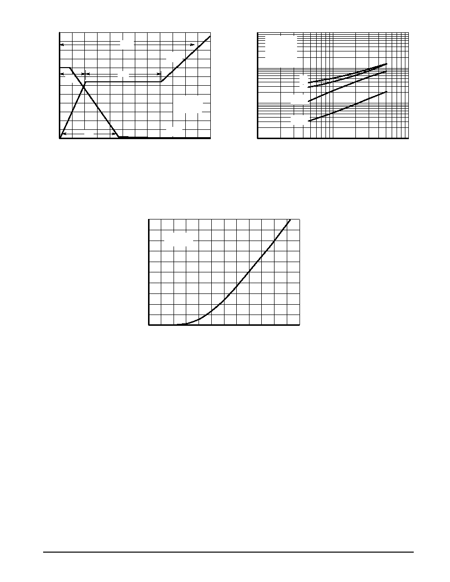
Figure 8. Gate Charge versus Gate–to–Source Voltage
I S
,SOURCE
CURRENT
(AMPS)
Figure 9. Resistive Switching Time
Variation versus Gate Resistance
RG, GATE RESISTANCE (OHMS)
t,
TIME
(ns)
Figure 10. Diode Forward Voltage versus Current
QT
TJ = 25°C
ID = 100 A
VDD = 50 V
ID = 100 A
VGS = 10 V
TJ = 25°C
td(on)
td(off)
tf
tr
0.9
100
250
80
60
40
20
1.1
1
Q1
Q3
VGS
VDS
SAFE OPERATING AREA
The Forward Biased Safe Operating Area curves define
the maximum simultaneous drain–to–source voltage and
drain current that a transistor can handle safely when it is for-
ward biased. Curves are based upon maximum peak junc-
tion temperature and a case temperature (TC) of 25°C. Peak
repetitive pulsed power limits are determined by using the
thermal response data in conjunction with the procedures
discussed in AN569, “Transient Thermal Resistance–General
Data and Its Use.”
Switching between the off–state and the on–state may tra-
verse any load line provided neither rated peak current (IDM)
nor rated voltage (VDSS) is exceeded and the transition time
(tr,tf) do not exceed 10 s. In addition the total power aver-
aged over a complete switching cycle must not exceed
(TJ(MAX) – TC)/(R
θJC).
A Power MOSFET designated E–FET can be safely used
in switching circuits with unclamped inductive loads. For reli-
able operation, the stored energy from circuit inductance dis-
sipated in the transistor while in avalanche must be less than
the rated limit and adjusted for operating conditions differing
from those specified. Although industry practice is to rate in
terms of energy, avalanche energy capability is not a con-
stant. The energy rating decreases non–linearly with an in-
crease of peak current in avalanche and peak junction
temperature.
Although many E–FETs can withstand the stress of drain–
to–source avalanche at currents up to rated pulsed current
(IDM), the energy rating is specified at rated continuous cur-
rent (ID), in accordance with industry custom. The energy rat-
ing must be derated for temperature as shown in the
accompanying graph (Figure 12). Maximum energy at cur-
rents below rated continuous ID can safely be assumed to
equal the values indicated.
相关PDF资料 |
PDF描述 |
|---|---|
| Y101132C203NQ | EZ-USB FX2LP™ USB Microcontroller High-Speed USB Peripheral Controller |
| Y1011U2C203NQ | 4-Mbit (256K x 16) Static RAM |
| Y201132C203NQ | SCHLUESSELSCHALTER EINE STELLUNGN DPCO |
| Y2011U2C203NQ | IC ASYN FIFO CASCA 32KX9 32-PLCC |
| Y1011U2AFWCNQE | 4, 5 & 6 Tumbler Switchlocks |
相关代理商/技术参数 |
参数描述 |
|---|---|
| Y100T | 制造商:SMC 功能描述:10 series compact T type spacer,6mm W |
| Y1011300203NQ | 制造商:C&K Components 功能描述: |
| Y101130A101NQ | 制造商:C&K Components 功能描述: |
| Y101130A103NQ | 制造商:C&K Components 功能描述: |
| Y101130D403QA | 制造商:C&K Components 功能描述: |
发布紧急采购,3分钟左右您将得到回复。