- 您现在的位置:买卖IC网 > PDF目录13597 > ZL2106ALCFTK (Intersil)IC REG BUCK SYNC ADJ 6A 36QFN PDF资料下载
参数资料
| 型号: | ZL2106ALCFTK |
| 厂商: | Intersil |
| 文件页数: | 11/29页 |
| 文件大小: | 0K |
| 描述: | IC REG BUCK SYNC ADJ 6A 36QFN |
| 标准包装: | 1,000 |
| 类型: | 降压(降压) |
| 输出类型: | 可调式 |
| 输出数: | 1 |
| 输出电压: | 0.54 V ~ 5.5 V |
| 输入电压: | 4.5 V ~ 14 V |
| PWM 型: | 电压模式 |
| 频率 - 开关: | 200kHz ~ 1MHz |
| 电流 - 输出: | 6A |
| 同步整流器: | 是 |
| 工作温度: | -40°C ~ 85°C |
| 安装类型: | 表面贴装 |
| 封装/外壳: | 36-VFQFN 裸露焊盘 |
| 包装: | 带卷 (TR) |
| 供应商设备封装: | 36-QFN |
第1页第2页第3页第4页第5页第6页第7页第8页第9页第10页当前第11页第12页第13页第14页第15页第16页第17页第18页第19页第20页第21页第22页第23页第24页第25页第26页第27页第28页第29页
�� �
�
�ZL2106�
�The� ZL2106� integrates� two� N-channel� power� MOSFETs;� QH� is� the�
�top� control� MOSFET� and� QL� is� the� bottom� synchronous� MOSFET.�
�The� amount� of� time� that� QH� is� on� as� a� fraction� of� the� total�
�switching� period� is� known� as� the� duty� cycle� D� ,� which� is� described�
�by� Equation� 1:�
�converted� to� a� digital� value� with� an� analog� to� digital� (A/D)�
�converter.� The� digital� signal� is� also� applied� to� an� adjustable�
�digital� compensation� filter� and� the� compensated� signal� is� used�
�to� derive� the� appropriate� PWM� duty� cycle� for� driving� the� internal�
�MOSFETs� in� a� way� that� produces� the� desired� output.�
�D� ≈�
�V� OUT�
�V� IN�
�(EQ.� 1)�
�Power� Management� Overview�
�The� ZL2106� incorporates� a� wide� range� of� configurable� power�
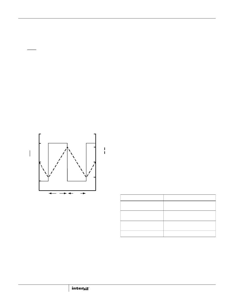
�During� time� D,� QH� is� on� and� V� IN� –� V� OUT� is� applied� across� the�
�inductor.� The� output� current� ramps� up� as� shown� in� Figure� 12.�
�When� QH� turns� off� (time� 1-D),� the� current� flowing� in� the� inductor�
�must� continue� to� flow� from� the� ground� up� through� QL,� during� which�
�the� current� ramps� down.� Since� the� output� capacitor� C� OUT� exhibits�
�low� impedance� at� the� switching� frequency,� the� AC� component� of� the�
�inductor� current� is� filtered� from� the� output� voltage� so� the� load� sees�
�nearly� a� DC� voltage.�
�The� maximum� conversion� ratio� is� shown� in� Figure� 9.� Typically,�
�buck� converters� specify� a� maximum� duty� cycle� that� effectively�
�limits� the� maximum� output� voltage� that� can� be� realized� for� a�
�given� input� voltage� and� switching� frequency.� This� duty� cycle� limit�
�ensures� that� the� low-side� MOSFET� is� allowed� to� turn� on� for� a�
�minimum� amount� of� time� during� each� switching� cycle,� which�
�enables� the� bootstrap� capacitor� to� be� charged� up� and� provide�
�adequate� gate� drive� voltage� for� the� high-side� MOSFET.�
�management� features� that� are� simple� to� implement� without�
�additional� components.� Also,� the� ZL2106� includes� circuit� protection�
�features� that� continuously� safeguard� the� device� and� load� from�
�damage� due� to� unexpected� system� faults.� The� ZL2106� can�
�continuously� monitor� input� voltage,� output� voltage/current� and�
�internal� temperature.� A� Power-good� output� signal� is� also� included� to�
�enable� power-on� reset� functionality� for� an� external� processor.�
�All� power� management� functions� can� be� configured� using� either�
�pin� configuration� techniques� (see� Figure� 13)� or� via� the�
�I� 2� C/SMBus� interface.� Monitoring� parameters� can� also� be�
�pre-configured� to� provide� alerts� for� specific� conditions.� See�
�Application� Note� AN2033� for� more� details� on� SMBus� monitoring.�
�Multi-mode� Pins�
�In� order� to� simplify� circuit� design,� the� ZL2106� incorporates�
�patented� multi-mode� pins� that� allow� the� user� to� easily� configure�
�many� aspects� of� the� device� without� programming.� Most� power�
�management� features� can� be� configured� using� these� pins.� The�
�multi-mode� pins� can� respond� to� four� different� connections,� as�
�V� IN� -� V� OUT�
�0�
�-V� OUT�
�D�
�1-D�
�IL� PK�
�I� O�
�IL� V�
�shown� in� Table� 1.� These� pins� are� sampled� when� power� is� applied�
�or� by� issuing� a� PMBus� Restore� command� (See� Application� Note�
�AN2033).�
�PIN-STRAP� SETTINGS�
�This� is� the� simplest� method,� as� no� additional� components� are�
�required.� Using� this� method,� each� pin� can� take� on� one� of� three�
�possible� states:� LOW,� OPEN,� or� HIGH.� These� pins� can� be�
�connected� to� the� V2P5� pin� for� logic� HIGH� settings� as� this� pin�
�provides� a� regulated� voltage� higher� than� 2V.� Using� a� single� pin�
�one� of� three� settings� can� be� selected.�
�TABLE� 1.� MULTI-MODE� PIN� CONFIGURATION�
�Time�
�FIGURE� 12.� INDUCTOR� WAVEFORM�
�In� general,� the� size� of� components� L� 1� and� C� OUT� as� well� as� the�
�overall� efficiency� of� the� circuit� are� inversely� proportional� to� the�
�switching� frequency,� f� SW� .� Therefore,� the� highest� efficiency� circuit�
�may� be� realized� by� switching� the� MOSFETs� at� the� lowest� possible�
�frequency;� however,� this� will� result� in� the� largest� component� size.�
�Conversely,� the� smallest� possible� footprint� may� be� realized� by�
�switching� at� the� fastest� possible� frequency� but� this� gives� a�
�somewhat� lower� efficiency.� Each� user� should� determine� the�
�optimal� combination� of� size� and� efficiency� when� determining� the�
�switching� frequency� for� each� application.�
�The� block� diagram� for� the� ZL2106� is� illustrated� in�
�Figure� 11.� In� this� circuit,� the� target� output� voltage� is� regulated� by�
�connecting� the� VSEN� pin� directly� to� the� output� regulation� point.�
�The� VSEN� signal� is� then� compared� to� an� internal� reference�
�voltage� that� had� been� set� to� the� desired� output� voltage� level� by�
�the� user.� The� error� signal� derived� from� this� comparison� is�
�11�
�PIN� TIED� TO�
�LOW�
�(Logic� LOW)�
�OPEN�
�(N/C)�
�HIGH�
�(Logic� HIGH)�
�Resistor� to� SGND�
�VALUE�
�<� 0.8VDC�
�No� connection�
�>� 2.0VDC�
�Set� by� resistor� value�
�FN6852.6�
�February� 20,� 2013�
�相关PDF资料 |
PDF描述 |
|---|---|
| ABM10DRTS | CONN EDGECARD 20POS DIP .156 SLD |
| ZL2106ALCFT | IC REG BUCK SYNC ADJ 6A 36QFN |
| ISL8033IRZ-T | IC REG BUCK SYNC ADJ 3A DL 24QFN |
| 16RX30680MT810X16 | CAP ALUM 680UF 16V 20% RADIAL |
| UPM1J100MDD | CAP ALUM 10UF 63V 20% RADIAL |
相关代理商/技术参数 |
参数描述 |
|---|---|
| ZL2106ALCFTR5520 | 制造商:Intersil Corporation 功能描述:6A DIGITAL DC-DC CONVERTER W/ DDC - TR4K - Tape and Reel |
| ZL2106ALCN | 功能描述:IC REG BUCK SYNC ADJ 6A 36QFN RoHS:是 类别:集成电路 (IC) >> PMIC - 稳压器 - DC DC 开关稳压器 系列:- 产品培训模块:Lead (SnPb) Finish for COTS Obsolescence Mitigation Program 标准包装:1 系列:- 类型:降压(降压) 输出类型:固定 输出数:1 输出电压:3.3V 输入电压:4.5 V ~ 24 V PWM 型:- 频率 - 开关:- 电流 - 输出:125mA 同步整流器:无 工作温度:-40°C ~ 85°C 安装类型:表面贴装 封装/外壳:SOT-23-6 包装:Digi-Reel® 供应商设备封装:SOT-6 其它名称:MAX1836EUT33#TG16DKR |
| ZL2106ALCNT | 功能描述:IC REG BUCK SYNC ADJ 6A 36QFN RoHS:是 类别:集成电路 (IC) >> PMIC - 稳压器 - DC DC 开关稳压器 系列:- 产品培训模块:Lead (SnPb) Finish for COTS Obsolescence Mitigation Program 标准包装:1 系列:- 类型:降压(降压) 输出类型:固定 输出数:1 输出电压:3.3V 输入电压:4.5 V ~ 24 V PWM 型:- 频率 - 开关:- 电流 - 输出:125mA 同步整流器:无 工作温度:-40°C ~ 85°C 安装类型:表面贴装 封装/外壳:SOT-23-6 包装:Digi-Reel® 供应商设备封装:SOT-6 其它名称:MAX1836EUT33#TG16DKR |
| ZL2106ALCNTK | 功能描述:IC REG BUCK SYNC ADJ 6A 36QFN RoHS:是 类别:集成电路 (IC) >> PMIC - 稳压器 - DC DC 开关稳压器 系列:- 产品培训模块:Lead (SnPb) Finish for COTS Obsolescence Mitigation Program 标准包装:1 系列:- 类型:降压(降压) 输出类型:固定 输出数:1 输出电压:3.3V 输入电压:4.5 V ~ 24 V PWM 型:- 频率 - 开关:- 电流 - 输出:125mA 同步整流器:无 工作温度:-40°C ~ 85°C 安装类型:表面贴装 封装/外壳:SOT-23-6 包装:Digi-Reel® 供应商设备封装:SOT-6 其它名称:MAX1836EUT33#TG16DKR |
| ZL2106EVAL1Z | 功能描述:BOARD EVAL STEP-DOWN ZL2106 RoHS:是 类别:编程器,开发系统 >> 评估板 - DC/DC 与 AC/DC(离线)SMPS 系列:Zilker Labs™ 产品培训模块:Obsolescence Mitigation Program 标准包装:1 系列:True Shutdown™ 主要目的:DC/DC,步升 输出及类型:1,非隔离 功率 - 输出:- 输出电压:- 电流 - 输出:1A 输入电压:2.5 V ~ 5.5 V 稳压器拓扑结构:升压 频率 - 开关:3MHz 板类型:完全填充 已供物品:板 已用 IC / 零件:MAX8969 |
发布紧急采购,3分钟左右您将得到回复。