- 您现在的位置:买卖IC网 > PDF目录17319 > ZL9101EVAL1Z (Intersil)EVALUATION BOARD 1 ZL9101 PDF资料下载
参数资料
| 型号: | ZL9101EVAL1Z |
| 厂商: | Intersil |
| 文件页数: | 14/19页 |
| 文件大小: | 0K |
| 描述: | EVALUATION BOARD 1 ZL9101 |
| 标准包装: | 1 |
| 主要目的: | DC/DC,步降 |
| 输出及类型: | 1,非隔离 |
| 输出电压: | 0.6 ~ 4 V |
| 电流 - 输出: | 12A |
| 输入电压: | 12V |
| 稳压器拓扑结构: | 降压 |
| 频率 - 开关: | 615kHz |
| 板类型: | 完全填充 |
| 已供物品: | 板 |
| 已用 IC / 零件: | ZL9101 |
�� �
�
�ZL9101M�
�Please� refer� to� Application� Note� AN2033� for� details� on� how� to�
�monitor� specific� parameters� via� the� I� 2� C/SMBus� interface.�
�Snapshot� Parameter� Capture�
�The� ZL9101M� offers� a� special� feature� that� enables� the� user� to�
�capture� parametric� data� during� normal� operation� or� following� a�
�fault.� The� SnapShot� functionality� is� enabled� by� setting� bit� 1� of�
�MISC_CONFIG� to� 1.�
�See� AN2033� for� details� on� using� SnapShot� in� addition� to� the�
�parameters� supported.� The� SnapShot� feature� enables� the� user� to�
�read� parameters� via� a� block� read� transfer� through� the� SMBus.�
�This� can� be� done� during� normal� operation,� although� it� should� be�
�noted� that� reading� the� 22� bytes� occupies� the� SMBus� for� some�
�time.�
�The� SNAPSHOT_CONTROL� command� enables� the� user� to� store�
�the� SnapShot� parameters� to� Flash� memory� in� response� to� a�
�pending� fault,� as� well� as� to� read� the� stored� data� from� Flash�
�memory� after� a� fault� has� occurred.� Table� 3� describes� the� usage�
�of� this� command.� Automatic� writes� to� Flash� memory� following� a�
�fault� are� triggered� when� any� fault� threshold� level� is� exceeded,�
�provided� that� the� specific� fault’s� response� is� to� shut� down�
�(writing� to� Flash� memory� is� not� allowed� if� the� device� is� configured�
�to� re-try� following� the� specific� fault� condition).� It� should� also� be�
�noted� that� the� module’s� V� DD� voltage� must� be� maintained� during�
�the� time� when� the� controller� is� writing� the� data� to� Flash� memory;�
�a� process� that� requires� between� 700μs� to� 1400μs,� depending� on�
�whether� the� data� is� set� up� for� a� block� write.� Undesirable� results�
�may� be� observed� if� the� device’s� V� DD� supply� drops� below� 3.0V�
�during� this� process.�
�TABLE� 3.� SNAPSHOT_CONTROL� COMMAND�
�DATA�
�1.� Default� Store:� The� ZL9101M� has� a� default� configuration� that� is�
�stored� in� the� default� store� in� the� controller.� The� module� can� be�
�restored� to� its� default� settings� by� issuing� a�
�RESTORE_DEFAULT_ALL� command� over� the� SMBus.�
�2.� User� Store:� The� user� can� modify� certain� power� supply� settings�
�as� described� in� this� data� sheet.� The� user� stores� their�
�configuration� in� the� user� store.�
�Please� refer� to� Application� Note� AN2033� for� details� on� how� to� set�
�specific� security� measures� via� the� I� 2� C/SMBus� interface.�
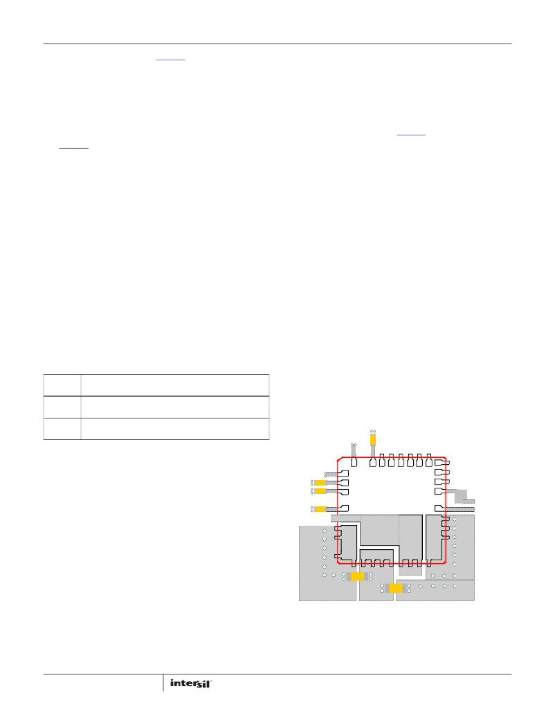
�Layout� Guide�
�To� achieve� stable� operation,� low� losses,� and� good� thermal�
�performance� some� layout� considerations� are� necessary�
�(Figure� 16).�
�?� Establish� a� continuous� ground� plane� connecting� SGND� (pin� 9),�
�PGND� (pin� 10),� and� PGND� (pin� 16).�
�?� Place� a� high� frequency� ceramic� capacitor� between� (1)� VIN� and�
�PGND� (pin� 16),� (2)� VOUT� and� PGND� (pin� 16)� and� (3)� bypass�
�capacitors� between� VDRV,� VDD,� V25,� VR� and� the� ground� plane,�
�as� close� to� the� module� as� possible� to� minimize� high� frequency�
�noise.� High� frequency� ceramic� capacitors� close� to� the� module�
�between� VOUT� and� PGND� will� help� to� minimize� noise� at� the�
�output� ripple.�
�?� Use� large� copper� areas� for� power� path� (VIN,� PGND,� VOUT)� to�
�minimize� conduction� loss� and� thermal� stress.� Also,� use�
�multiple� vias� to� connect� the� power� planes� in� different� layers.�
�?� Connect� remote� sensed� traces� to� the� regulation� point� to�
�achieve� a� tight� output� voltage� regulation,� and� keep� them� in�
�parallel.� Route� a� trace� from� FB-� to� a� location� near� the� load�
�ground,� and� a� trace� from� FB+� to� the� point-of-load� where� the�
�tight� output� voltage� is� desired.�
�VALUE�
�1�
�2�
�DESCRIPTION�
�Copies� current� SNAPSHOT� values� from� Flash� memory� to�
�RAM� for� immediate� access� using� SNAPSHOT� command.�
�Writes� current� SNAPSHOT� values� to� Flash� memory.� Only�
�available� when� device� is� disabled.�
�?� Avoid� routing� any� sensitive� signal� traces,� such� as� the� VOUT,�
�FB+,� FB-� sensing� point� near� the� PHASE� pin.�
�CVR�
�If� the� module� experiences� a� fault� and� power� is� lost,� the� user� can�
�extract� the� last� SnapShot� parameters� stored� during� the� fault� by�
�9�
�8�
�7�
�6�
�5�
�4�
�3�
�2�
�1�
�SDA�
�writing� a� 1� to� SNAPSHOT_CONTROL� (transfers� data� from� Flash�
�PGND�
�10�
�2� 1�
�VSET�
�memory� to� RAM)� and� then� issuing� a� SNAPSHOT� command� (reads�
�data� from� RAM� via� SMBus).�
�Non-Volatile� Memory� and� Device� Security�
�CV25�
�CVDD�
�CVDRV�
�V25�
�VDD�
�VDRV�
�11�
�12�
�13�
�2� 0�
�1� 9�
�18�
�VTRK�
�FB+�
�FB-�
�TO�
�VOUT�
�TO�
�LOAD� GND�
�Features�
�SW�
�The� ZL9101M� has� internal� non-volatile� memory� where� user�
�configurations� are� stored.� Integrated� security� measures� ensure�
�that� the� user� can� only� restore� the� module� to� a� level� that� has� been�
�VIN�
�15�
�PGND�
�1� 6�
�14�
�VOUT�
�17�
�made� available� to� them.�
�During� the� initialization� process,� the� ZL9101M� checks� for� stored�
�values� contained� in� its� internal� non-volatile� memory.� The�
�ZL9101M� offers� two� internal� memory� storage� units� that� are�
�accessible� by� the� user� as� follows:�
�14�
�CIN�
�COUT�
�FIGURE� 16.� RECOMMENDED� LAYOUT�
�FN7669.4�
�January� 20,� 2012�
�相关PDF资料 |
PDF描述 |
|---|---|
| GEC19DREN-S13 | CONN EDGECARD 38POS .100 EXTEND |
| GEC19DREH-S13 | CONN EDGECARD 38POS .100 EXTEND |
| EEC19DRTS-S13 | CONN EDGECARD 38POS .100 EXTEND |
| EBC10DRTI-S13 | CONN EDGECARD 20POS .100 EXTEND |
| EEC19DRES-S13 | CONN EDGECARD 38POS .100 EXTEND |
相关代理商/技术参数 |
参数描述 |
|---|---|
| ZL9101M | 制造商:INTERSIL 制造商全称:Intersil Corporation 功能描述:Digital DC/DC PMBus 12A Module |
| ZL9101M_11 | 制造商:INTERSIL 制造商全称:Intersil Corporation 功能描述:Digital DC/DC PMBus 12A Module |
| ZL9101M_1104 | 制造商:INTERSIL 制造商全称:Intersil Corporation 功能描述:Digital DC/DC PMBus 12A Module |
| ZL9101MIRZ | 功能描述:MODULE DGTL DC-DC 12A 21QFN RoHS:是 类别:电源 - 板载 >> DC DC Converters 系列:ZL9101M 标准包装:15 系列:Econoline REC3-DR 类型:隔离 输出数:2 电压 - 输入(最小):4.5V 电压 - 输入(最大):5.5V Voltage - Output 1:5V Voltage - Output 2:-5V Voltage - Output 3:- 电流 - 输出(最大):300mA,300mA 电源(瓦) - 制造商系列:3W 电压 - 隔离:1kV(1000V) 特点:- 安装类型:表面贴装 封装/外壳:24-DIP SMD 模块(18 引线) 尺寸/尺寸:1.26" L x 0.80" W x 0.44" H(32.0mm x 20.3mm x 11.2mm) 包装:管件 工作温度:-40°C ~ 80°C 效率:75% 电源(瓦特)- 最大:3W 其它名称:10005457 |
| ZL9101MIRZ-T | 功能描述:DCDC DGTL PMBUS MODULE 12A 21QFN RoHS:是 类别:电源 - 板载 >> DC DC Converters 系列:ZL9101M 标准包装:10 系列:PT4570 类型:隔离 输出数:1 电压 - 输入(最小):36V 电压 - 输入(最大):75V Voltage - Output 1:9V Voltage - Output 2:- Voltage - Output 3:- 电流 - 输出(最大):3.3A 电源(瓦) - 制造商系列:30W 电压 - 隔离:1.5kV(1500V) 特点:- 安装类型:表面贴装 封装/外壳:19-SIP SMD 模块 尺寸/尺寸:3.00" L x 1.19" W x 0.50" H(76.2mm x 30.2mm x 12.7mm) 包装:托盘 工作温度:-40°C ~ 85°C 效率:84% 电源(瓦特)- 最大:30W |
发布紧急采购,3分钟左右您将得到回复。