- 您现在的位置:买卖IC网 > PDF目录17319 > ZL9101EVAL1Z (Intersil)EVALUATION BOARD 1 ZL9101 PDF资料下载
参数资料
| 型号: | ZL9101EVAL1Z |
| 厂商: | Intersil |
| 文件页数: | 15/19页 |
| 文件大小: | 0K |
| 描述: | EVALUATION BOARD 1 ZL9101 |
| 标准包装: | 1 |
| 主要目的: | DC/DC,步降 |
| 输出及类型: | 1,非隔离 |
| 输出电压: | 0.6 ~ 4 V |
| 电流 - 输出: | 12A |
| 输入电压: | 12V |
| 稳压器拓扑结构: | 降压 |
| 频率 - 开关: | 615kHz |
| 板类型: | 完全填充 |
| 已供物品: | 板 |
| 已用 IC / 零件: | ZL9101 |
�� �
�
�ZL9101M�
�Thermal� Considerations�
�Experimental� power� loss� curves� along� with� θ� JA� from� thermal�
�modeling� analysis� can� be� used� to� evaluate� the� thermal�
�consideration� for� the� module.� The� derating� curves� are� derived�
�from� the� maximum� power� allowed� while� maintaining� the�
�temperature� below� the� maximum� junction� temperature� of�
�+125°C.� In� actual� application,� other� heat� sources� and� design�
�margin� should� be� considered.�
�Package� Description�
�The� structure� of� the� ZL9101M� belongs� to� the� Quad� Flat-pack�
�No-lead� package� (QFN).� This� kind� of� package� has� advantages,�
�such� as� good� thermal� and� electrical� conductivity,� low� weight� and�
�small� size.� The� QFN� package� is� applicable� for� surface� mounting�
�technology� and� is� being� more� readily� used� in� the� industry.� The�
�ZL9101M� contains� several� types� of� devices,� including� resistors,�
�capacitors,� inductors� and� control� ICs.� The� ZL9101M� is� a� copper�
�lead-frame� based� package� with� exposed� copper� thermal� pads,�
�which� have� good� electrical� and� thermal� conductivity.� The� copper�
�lead� frame� and� multi� component� assembly� is� overmolded� with�
�polymer� mold� compound� to� protect� these� devices.�
�The� package� outline� and� typical� PCB� layout� pattern� design� and�
�typical� stencil� pattern� design� are� shown� on� the� second� page� of�
�the� package� outline� drawing� L21.15x15� on� page� 18.� The� module�
�has� a� small� size� of� 15mm� x� 15mm� x� 3.5mm.� Figure� 17� shows�
�typical� reflow� profile� parameters.� These� guidelines� are� general�
�prevent� solder� bridging� between� adjacent� I/O� lands.� To� reduce�
�solder� paste� volume� on� the� larger� thermal� lands,� it� is�
�recommended� that� an� array� of� smaller� apertures� be� used� instead�
�of� one� large� aperture.� It� is� recommended� that� the� stencil� printing�
�area� cover� 50%� to� 80%� of� the� PCB� layout� pattern.� A� typical� solder�
�stencil� pattern� is� shown� on� the� second� page� of� the� Package�
�Outline� Drawing� L21.15x15� on� page� 18.� The� gap� width� between�
�pad� to� pad� is� 0.6mm.� The� user� should� consider� the� symmetry� of�
�the� whole� stencil� pattern� when� designing� its� pads.� A� laser� cut,�
�stainless� steel� stencil� with� electropolished� trapezoidal� walls� is�
�recommended.� Electropolishing� “smooths”� the� aperture� walls�
�resulting� in� reduced� surface� friction� and� better� paste� release� which�
�reduces� voids.� Using� a� Trapezoidal� Section� Aperture� (TSA)� also�
�promotes� paste� release� and� forms� a� "brick� like"� paste� deposit� that�
�assists� in� firm� component� placement.� A� 0.1mm� to� 0.15mm� stencil�
�thickness� is� recommended� for� this� large� pitch� (1.3mm)� QFN.�
�Reflow� Parameters�
�Due� to� the� low� mount� height� of� the� QFN,� "No� Clean"� Type� 3� solder�
�paste� per� ANSI/J-STD-005� is� recommended.� Nitrogen� purge� is�
�also� recommended� during� reflow.� A� system� board� reflow� profile�
�depends� on� the� thermal� mass� of� the� entire� populated� board,� so� it�
�is� not� practical� to� define� a� specific� soldering� profile� just� for� the�
�QFN.� The� profile� given� in� Figure� 17� is� provided� as� a� guideline,� to�
�be� customized� for� varying� manufacturing� practices� and�
�applications.�
�design� rules.� Users� could� modify� parameters� according� to� their�
�application.�
�PCB� Layout� Pattern� Design�
�The� bottom� of� ZL9101M� is� a� lead-frame� footprint,� which� is�
�attached� to� the� PCB� by� surface� mounting� process.� The� PCB�
�layout� pattern� is� shown� on� the� second� page� of� the� Package�
�Outline� Drawing� L21.15x15� on� page� 18.� The� PCB� layout� pattern� is�
�essentially� 1:1� with� the� QFN� exposed� pad� and� I/O� termination�
�dimensions,� except� for� the� PCB� lands� being� a� slightly� extended�
�distance� of� 0.2mm� (0.4mm� max)� longer� than� the� QFN�
�terminations,� which� allows� for� solder� filleting� around� the�
�periphery� of� the� package.� This� ensures� a� more� complete� and�
�300�
�250�
�200�
�150�
�100�
�50�
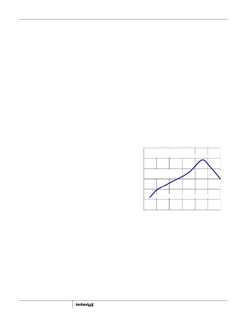
�PEAK� TEMPERATURE� ~+245°C;�
�TYPICALLY� 60s-150s� ABOVE� +217°C�
�KEEP� LESS� THAN� 30s� WITHIN 5°C OF PEAK TEMP.�
�SLOW� RAMP� (3°C/s� MAX)�
�AND� SOAK� FROM� +150°C�
�TO� +200°C� FOR� 60s~180s�
�RAMP RATE� ≤� 1.5°C FROM +70°C TO +90°C�
�inspectable� solder� joint.� The� thermal� lands� on� the� PCB� layout�
�should� match� 1:1� with� the� package� exposed� die� pads.�
�0�
�0�
�100�
�150�
�200�
�250�
�300�
�350�
�Thermal� Vias�
�A� grid� of� 1.0mm� to� 1.2mm� pitch� thermal� vias,� which� drops� down�
�and� connects� to� buried� copper� plane(s),� should� be� placed� under� the�
�thermal� land.� The� vias� should� be� about� 0.3mm� to� 0.33mm� in�
�diameter� with� the� barrel� plated� to� about� 1.0� ounce� copper.�
�Although� adding� more� vias� (by� decreasing� via� pitch)� will� improve�
�the� thermal� performance,� diminishing� returns� will� be� seen� as� more�
�and� more� vias� are� added.� Simply� use� as� many� vias� as� practical� for�
�the� thermal� land� size� and� your� board� design� rules� allow.�
�Stencil� Pattern� Design�
�Reflowed� solder� joints� on� the� perimeter� I/O� lands� should� have�
�about� a� 50μm� to� 75μm� (2mil� to� 3mil)� standoff� height.� The� solder�
�paste� stencil� design� is� the� first� step� in� developing� optimized,�
�reliable� solder� joins.� Stencil� aperture� size� to� land� size� ratio� should�
�typically� be� 1:1.� The� aperture� width� may� be� reduced� slightly� to� help�
�15�
�DURATION� (s)�
�FIGURE� 17.� TYPICAL� REFLOW� PROFILE�
�FN7669.4�
�January� 20,� 2012�
�相关PDF资料 |
PDF描述 |
|---|---|
| GEC19DREN-S13 | CONN EDGECARD 38POS .100 EXTEND |
| GEC19DREH-S13 | CONN EDGECARD 38POS .100 EXTEND |
| EEC19DRTS-S13 | CONN EDGECARD 38POS .100 EXTEND |
| EBC10DRTI-S13 | CONN EDGECARD 20POS .100 EXTEND |
| EEC19DRES-S13 | CONN EDGECARD 38POS .100 EXTEND |
相关代理商/技术参数 |
参数描述 |
|---|---|
| ZL9101M | 制造商:INTERSIL 制造商全称:Intersil Corporation 功能描述:Digital DC/DC PMBus 12A Module |
| ZL9101M_11 | 制造商:INTERSIL 制造商全称:Intersil Corporation 功能描述:Digital DC/DC PMBus 12A Module |
| ZL9101M_1104 | 制造商:INTERSIL 制造商全称:Intersil Corporation 功能描述:Digital DC/DC PMBus 12A Module |
| ZL9101MIRZ | 功能描述:MODULE DGTL DC-DC 12A 21QFN RoHS:是 类别:电源 - 板载 >> DC DC Converters 系列:ZL9101M 标准包装:15 系列:Econoline REC3-DR 类型:隔离 输出数:2 电压 - 输入(最小):4.5V 电压 - 输入(最大):5.5V Voltage - Output 1:5V Voltage - Output 2:-5V Voltage - Output 3:- 电流 - 输出(最大):300mA,300mA 电源(瓦) - 制造商系列:3W 电压 - 隔离:1kV(1000V) 特点:- 安装类型:表面贴装 封装/外壳:24-DIP SMD 模块(18 引线) 尺寸/尺寸:1.26" L x 0.80" W x 0.44" H(32.0mm x 20.3mm x 11.2mm) 包装:管件 工作温度:-40°C ~ 80°C 效率:75% 电源(瓦特)- 最大:3W 其它名称:10005457 |
| ZL9101MIRZ-T | 功能描述:DCDC DGTL PMBUS MODULE 12A 21QFN RoHS:是 类别:电源 - 板载 >> DC DC Converters 系列:ZL9101M 标准包装:10 系列:PT4570 类型:隔离 输出数:1 电压 - 输入(最小):36V 电压 - 输入(最大):75V Voltage - Output 1:9V Voltage - Output 2:- Voltage - Output 3:- 电流 - 输出(最大):3.3A 电源(瓦) - 制造商系列:30W 电压 - 隔离:1.5kV(1500V) 特点:- 安装类型:表面贴装 封装/外壳:19-SIP SMD 模块 尺寸/尺寸:3.00" L x 1.19" W x 0.50" H(76.2mm x 30.2mm x 12.7mm) 包装:托盘 工作温度:-40°C ~ 85°C 效率:84% 电源(瓦特)- 最大:30W |
发布紧急采购,3分钟左右您将得到回复。