- 您现在的位置:买卖IC网 > PDF目录19400 > ZY7007LG-T3 (Power-One)PROGBL CONVERT DC-DC 7A OUT SMD PDF资料下载
参数资料
| 型号: | ZY7007LG-T3 |
| 厂商: | Power-One |
| 文件页数: | 26/35页 |
| 文件大小: | 0K |
| 描述: | PROGBL CONVERT DC-DC 7A OUT SMD |
| 特色产品: | ZY Series Converters |
| 标准包装: | 1 |
| 系列: | 智能 POL 转换器 |
| 类型: | 非隔离(POL) |
| 输出数: | 1 |
| 电压 - 输入(最小): | 3V |
| 电压 - 输入(最大): | 14V |
| Voltage - Output 1: | 0.5 ~ 5.5 V |
| 电流 - 输出(最大): | 7A |
| 电源(瓦) - 制造商系列: | 38W |
| 安装类型: | 表面贴装 |
| 封装/外壳: | 36-DIP SMD 模块 |
| 尺寸/尺寸: | 0.87" L x 0.49" W x 0.26" H(22.2mm x 12.5mm x 6.5mm) |
| 包装: | 标准包装 |
| 工作温度: | -40°C ~ 85°C |
| 电源(瓦特)- 最大: | 38.5W |
| 产品目录页面: | 2739 (CN2011-ZH PDF) |
| 其它名称: | 179-2410-6 |
第1页第2页第3页第4页第5页第6页第7页第8页第9页第10页第11页第12页第13页第14页第15页第16页第17页第18页第19页第20页第21页第22页第23页第24页第25页当前第26页第27页第28页第29页第30页第31页第32页第33页第34页第35页
�� �
�
�ZY7007� 7A� DC-DC� Intelligent� POL� Data� Sheet�
�3V� to� 14V� Input� ?� 0.5V� to� 5.5V� Output�
�directly� via� the� I� 2� C� bus� by� writing� into� the� INT� register�
�shown� in� Figure� 46.� Note� that� the� content� of� the�
�register� can� be� changed� only� when� the� POL� is�
�turned� off.�
�R/W-0�
�FRQ2�
�Bit� 7�
�R/W-0�
�FRQ1�
�R/W-0�
�FRQ0�
�R/W-0� 1)�
�INT4�
�R/W-0� 1)�
�INT3�
�R/W-0� 1)�
�INT2�
�R/W-0� 1)�
�INT1�
�R/W-0� 1)�
�INT0�
�Bit� 0�
�Switching� actions� of� all� POLs� connected� to� the� SD�
�line� are� synchronized� to� the� master� clock� generated�
�by� the� DPM.� Each� POL� is� equipped� with� a� PLL� and�
�a� frequency� divider� so� they� can� operate� at� multiples�
�(including� fractional)� of� the� master� clock� frequency�
�as� programmed� by� a� user.� The� POL� converters� can�
�Bit� 7:5� FRQ[2:0]� :� PWM� Frequency� Selection�
�000:� 500kHz�
�001:� 750kHz�
�010:� 1000lHz�
�011:� 1250kHz�
�100:� 1250kHz�
�101:� 1500kHz�
�110:� 1750kHz�
�111:� 2000kHz�
�Bit� 4:0� INT[4:0]� :� Interleave� position�
�R� =� Readable� bit�
�W� =� Writable� bit�
�U� =� Unimplemented� bit,�
�read� as� ‘0’�
�-� n� =� Value� at� POR� reset�
�operate� at� 500� kHz,� 750� kHz,� and� 1� MHz.� Although�
�synchronized,� switching� frequencies� of� different�
�POLs� are� independent� of� each� other.� It� is�
�permissible� to� mix� POLs� operating� at� different�
�frequencies� in� one� system.� It� allows� optimizing�
�efficiency� and� transient� response� of� each� POL� in� the�
�system� individually.�
�1)�
�00h:� Ton� starts� with� 0.0°� Phase� lag� to� SD� Line�
�01h:� Ton� starts� wi� th� 11.25°� Phase� lag� to� SD� Line�
�02h:� Ton� starts� with� 22.50°� Phase� lag� to� SD� Line�
�…�
�1Fh:� Ton� starts� with� 348.75°� Phase� lag� to� SD� Line�
�Initial� value� depends� on� the� state� of� the� Interleave� Mode� (� IM� )� Input:�
�IM=Open:� At� POR� reset� the� 5� corresponding� ADDRESS� bits� are� loaded�
�IM=Low:� At� POR� reset� a� 0� is� loaded�
�Figure� 46.� Interleave� Configuration� Register� INT�
�8.4.2� Interleave�
�Interleave� is� defined� as� a� phase� delay� between� the�
�synchronizing� slope� of� the� master� clock� on� the� SD�
�pin� and� PWM� signal� of� a� POL.� The� interleave� can�
�be� programmed� in� the� GUI� PWM� Controller� window�
�or� directly� via� the� I� 2� C� bus� by� writing� into� the� INT�
�register.�
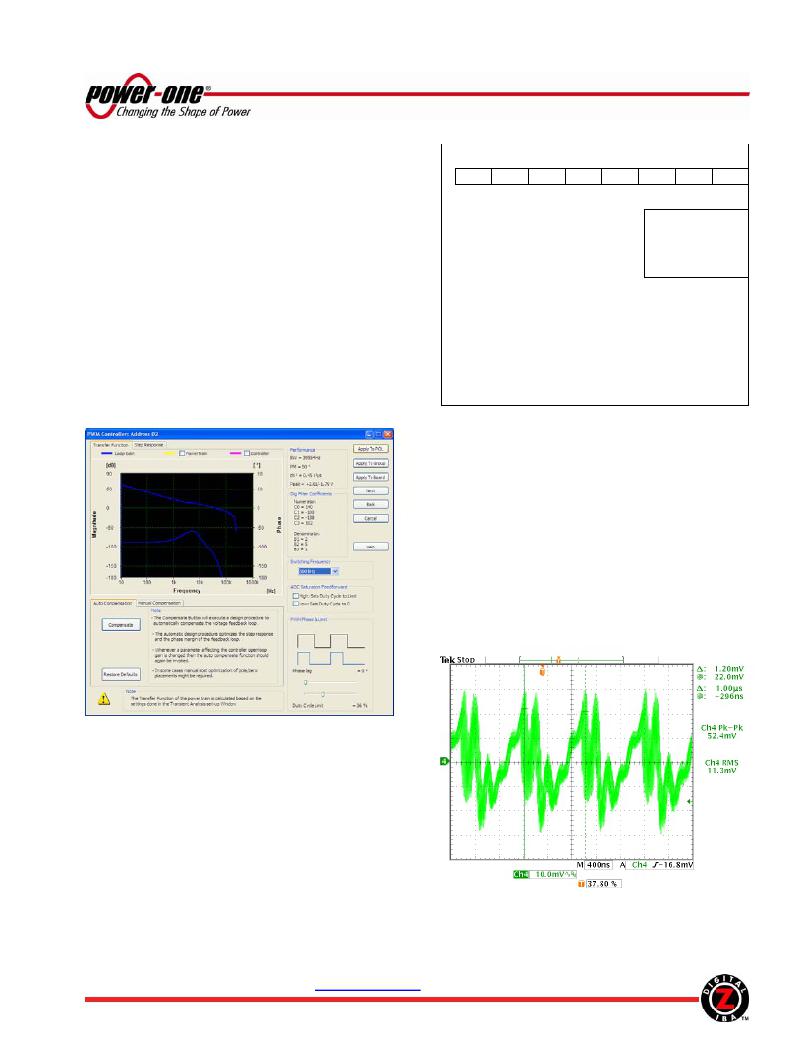
�Every� POL� generates� switching� noise.� If� no�
�interleave� is� programmed,� all� POLs� in� the� system�
�switch� simultaneously� and� noise� reflected� to� the�
�input� source� from� all� POLs� is� added� together� as�
�shown� in� Figure� 47.�
�Figure� 45.� PWM� Controller� Window�
�Figure� 47.� Input� Voltage� Noise,� No� Interleave�
�ZD-00245� Rev.� 2.6,� 01-Jul-10�
�www.power-one.com�
�Page� 26� of� 35�
�相关PDF资料 |
PDF描述 |
|---|---|
| VI-23B-CY-F1 | CONVERTER MOD DC/DC 95V 50W |
| MAX7503MSA+T | IC TEMP SENSOR DIGIT 8-SOIC |
| ADSP-BF514KBCZ-4 | IC DSP 16/32B 400MHZ 168CSPBGA |
| VI-233-CY-F3 | CONVERTER MOD DC/DC 24V 50W |
| LSM2-T/6-D12-C | CONV DC/DC 30W 6A 12V SMD |
相关代理商/技术参数 |
参数描述 |
|---|---|
| ZY7007L-T3 | 制造商:Power-One 功能描述:- Tape and Reel |
| ZY7007LU-Q1 | 制造商:POWER-ONE 制造商全称:Power-One 功能描述:7A DC-DC Intelligent POL 3V to 14V Input - 0.5V to 5.5V Output |
| ZY7007LU-T1 | 制造商:POWER-ONE 制造商全称:Power-One 功能描述:7A DC-DC Intelligent POL 3V to 14V Input - 0.5V to 5.5V Output |
| ZY7007LU-T2 | 制造商:POWER-ONE 制造商全称:Power-One 功能描述:7A DC-DC Intelligent POL 3V to 14V Input - 0.5V to 5.5V Output |
| ZY7007LU-T3 | 制造商:POWER-ONE 制造商全称:Power-One 功能描述:7A DC-DC Intelligent POL 3V to 14V Input - 0.5V to 5.5V Output |
发布紧急采购,3分钟左右您将得到回复。