- 您现在的位置:买卖IC网 > PDF目录155701 > 24LCS61/ST 128 X 8 I2C/2-WIRE SERIAL EEPROM, PDSO8 PDF资料下载
参数资料
| 型号: | 24LCS61/ST |
| 元件分类: | PROM |
| 英文描述: | 128 X 8 I2C/2-WIRE SERIAL EEPROM, PDSO8 |
| 封装: | TSSOP-8 |
| 文件页数: | 14/17页 |
| 文件大小: | 249K |
| 代理商: | 24LCS61/ST |
24LCS61/62
DS21226C-page 6
Preliminary
1999 Microchip Technology Inc.
4.0
FUNCTIONAL DESCRIPTION
The 24LCS61/62 supports a bi-directional 2-wire bus
and data transmission protocol compatible with the I2C
protocol. The device is configured to reside on a com-
mon I2C bus with up to 255 total 24LCS61/62 devices
on the bus. Each device has a unique serial number
assigned to it when delivered from the factory. In an
actual system, this serial number will be used to assign
a separate 8-bit ID byte to each device in the system.
After an ID byte is assigned to each device in the sys-
tem, standard read and write commands can be sent to
each device individually.
4.1
Device Serial Number
The device serial number is stored in a 48-bit (6 byte)
register that is separate from the data array. The serial
number register is non-volatile and cannot be changed
by the user. Before shipment from the factory, this reg-
ister is programmed with a unique value for every
device. The 48 bit register allows for 2.8
1014 different
combinations. The serial number is used at power-up to
assign the device an ID byte which is then used for all
standard read and write commands sent to that specific
device.
4.2
Device ID Byte
The Device ID byte is an 8-bit value that provides the
means for every device on the bus to be accessed indi-
vidually. The ID byte is stored in a RAM register sepa-
rate from the data array. The ID byte register will always
default to address 00 upon power-up.
4.3
Device Addressing
Each command to the device must begin with a start
bit. A control byte is the first byte received following the
start condition from the master device (Figure 4-1). The
control byte consists of a four-bit control code, the OE
bit, and three command select bits. For the 24LCS61/
62, the control code is set to 0110 binary for all opera-
tions. The device will not acknowledge any commands
sent with any other control code. The next bit is the Out-
put Enable (OE) bit. This bit controls the operation of
the EDS pin. See Section 9.0 for more details. The last
three bits of the control byte are the command select
bits (C0-C2). The command select bits determine
which command will be executed. See Table 4-1. Fol-
lowing a valid control byte, the 24LCS61/62 will
acknowledge the command.
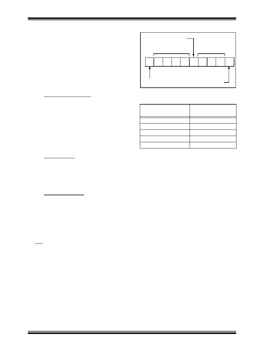
FIGURE 4-1:
CONTROL BYTE FORMAT
TABLE 4-1:
COMMAND CODES
Command
Command Select Bits
(C2 C1 C0)
Set Write Protection Fuse
000
Read
001
Write (Byte or Page)
010
Assign Address
100
Clear Address
110
1
01
0
OE
C2
C1
SACK
Control Code
Command Select
Bits
Acknowledge Bit
Start Bit
C0
Output Enable
Bit
相关PDF资料 |
PDF描述 |
|---|---|
| 24PCCFA6A | ABSOLUTE, PEIZORESISTIVE PRESSURE SENSOR, 2-15Psi, -16-(-216)mV, RECTANGULAR, THROUGH HOLE MOUNT |
| 24PCDFA6A | ABSOLUTE, PEIZORESISTIVE PRESSURE SENSOR, 0-30Psi, RECTANGULAR, THROUGH HOLE MOUNT |
| 24PCT130TO5(N) | T-1 SINGLE COLOR LED, ORANGE, 3 mm |
| 21PCT110CWLY5 | T-1 SINGLE COLOR LED, LIME YELLOW, 3 mm |
| 21PCT110CWR400 | T-1 SINGLE COLOR LED, ULTRA RED, 3 mm |
相关代理商/技术参数 |
参数描述 |
|---|---|
| 24LCS61T/SN | 功能描述:电可擦除可编程只读存储器 128x8 RoHS:否 制造商:Atmel 存储容量:2 Kbit 组织:256 B x 8 数据保留:100 yr 最大时钟频率:1000 KHz 最大工作电流:6 uA 工作电源电压:1.7 V to 5.5 V 最大工作温度:+ 85 C 安装风格:SMD/SMT 封装 / 箱体:SOIC-8 |
| 24LCS61T/ST | 功能描述:电可擦除可编程只读存储器 128x8 RoHS:否 制造商:Atmel 存储容量:2 Kbit 组织:256 B x 8 数据保留:100 yr 最大时钟频率:1000 KHz 最大工作电流:6 uA 工作电源电压:1.7 V to 5.5 V 最大工作温度:+ 85 C 安装风格:SMD/SMT 封装 / 箱体:SOIC-8 |
| 24LCS61T-I/SN | 功能描述:电可擦除可编程只读存储器 128x8 RoHS:否 制造商:Atmel 存储容量:2 Kbit 组织:256 B x 8 数据保留:100 yr 最大时钟频率:1000 KHz 最大工作电流:6 uA 工作电源电压:1.7 V to 5.5 V 最大工作温度:+ 85 C 安装风格:SMD/SMT 封装 / 箱体:SOIC-8 |
| 24LCS61T-I/ST | 功能描述:电可擦除可编程只读存储器 128x8 RoHS:否 制造商:Atmel 存储容量:2 Kbit 组织:256 B x 8 数据保留:100 yr 最大时钟频率:1000 KHz 最大工作电流:6 uA 工作电源电压:1.7 V to 5.5 V 最大工作温度:+ 85 C 安装风格:SMD/SMT 封装 / 箱体:SOIC-8 |
| 24LCS62/P | 功能描述:电可擦除可编程只读存储器 256x8 RoHS:否 制造商:Atmel 存储容量:2 Kbit 组织:256 B x 8 数据保留:100 yr 最大时钟频率:1000 KHz 最大工作电流:6 uA 工作电源电压:1.7 V to 5.5 V 最大工作温度:+ 85 C 安装风格:SMD/SMT 封装 / 箱体:SOIC-8 |
发布紧急采购,3分钟左右您将得到回复。