- 您现在的位置:买卖IC网 > Datasheet目录377 > 2N7002DW-7 (Diodes Inc)MOSFET N-CHANEL DUAL 60V SOT-363 Datasheet资料下载
参数资料
| 型号: | 2N7002DW-7 |
| 厂商: | Diodes Inc |
| 文件页数: | 2/5页 |
| 文件大小: | 0K |
| 描述: | MOSFET N-CHANEL DUAL 60V SOT-363 |
| 标准包装: | 1 |
| FET 型: | 2 个 N 沟道(双) |
| FET 特点: | 逻辑电平门 |
| 漏极至源极电压(Vdss): | 60V |
| 电流 - 连续漏极(Id) @ 25° C: | 115mA |
| 开态Rds(最大)@ Id, Vgs @ 25° C: | 7.5 欧姆 @ 50mA,5V |
| Id 时的 Vgs(th)(最大): | 2V @ 250µA |
| 输入电容 (Ciss) @ Vds: | 50pF @ 25V |
| 功率 - 最大: | 200mW |
| 安装类型: | 表面贴装 |
| 封装/外壳: | 6-TSSOP,SC-88,SOT-363 |
| 供应商设备封装: | SOT-363 |
| 包装: | 剪切带 (CT) |
| 其它名称: | 2N7002DWDICT |
�� �
�
�2N7002DW�
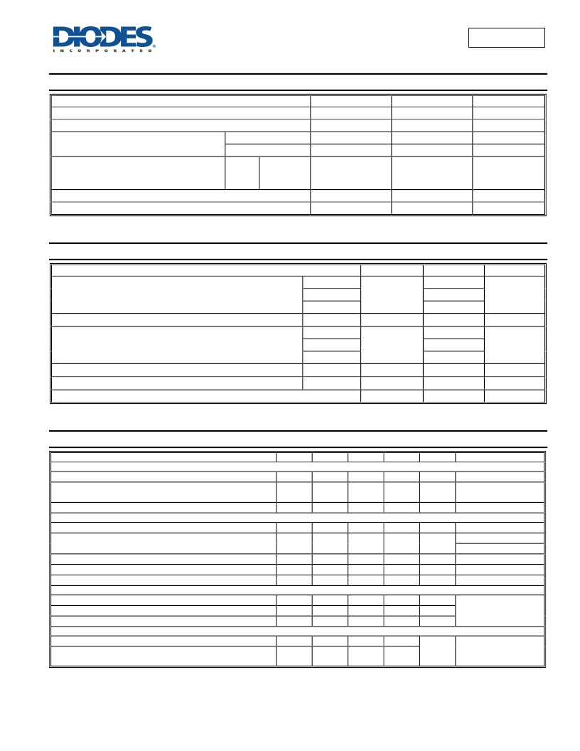
�Maximum� Ratings� (@T� A� =� +25°C,� unless� otherwise� specified.)�
�Characteristic�
�Drain-Source� Voltage�
�Drain-Gate� Voltage� R� GS� ≤� 1.0M� Ω�
�Symbol�
�V� DSS�
�V� DGR�
�Value�
�60�
�60�
�Units�
�V�
�V�
�Gate-Source� Voltage�
�Continuous�
�Pulsed�
�V� GSS�
�V� GSS�
�±20�
�±40�
�V�
�V�
�Continuous� Drain� Current� (Note� 7)� V� GS� =� 5V�
�Steady�
�State�
�T� A� =� +25� °� C�
�T� A� =� +70� °� C�
�T� A� =� +100� °� C�
�I� D�
�0.23�
�0.18�
�0.14�
�A�
�Maximum� Continuous� Body� Diode� Forward� Current� (Note� 7)�
�Pulsed� Drain� Current� (10μs� pulse,� duty� cycle� =� 1%)�
�I� S�
�I� DM�
�0.53�
�0.8�
�A�
�A�
�Thermal� Characteristics� (@T� A� =� +25°C,� unless� otherwise� specified.)�
�Characteristic�
�T� A� =� +25°C�
�Symbol�
�Value�
�0.31�
�Units�
�Total� Power� Dissipation� (Note� 6)�
�T� A� =� +70°C�
�P� D�
�0.2�
�W�
�T� A� =� +100°C�
�0.12�
�Thermal� Resistance,� Junction� to� Ambient� (Note� 6)�
�Steady� state�
�R� θ� JA�
�410�
�°C/W�
�T� A� =� +25°C�
�0.4�
�Total� Power� Dissipation� (Note� 7)�
�T� A� =� +70°C�
�P� D�
�0.25�
�W�
�T� A� =� +100°C�
�0.15�
�Thermal� Resistance,� Junction� to� Ambient� (Note� 7)�
�Thermal� Resistance,� Junction� to� Case� (Note� 7)�
�Operating� and� Storage� Temperature� Range�
�Steady� state�
�Steady� state�
�R� θ� JA�
�R� θ� JC�
�T� J,� T� STG�
�318�
�135�
�-55� to� +150�
�°C/W�
�°C/W�
�°C�
�Electrical� Characteristics� (@T� A� =� +25°C,� unless� otherwise� specified.)�
�Characteristic�
�Symbol�
�Min�
�Typ�
�Max�
�Unit�
�Test� Condition�
�OFF� CHARACTERISTICS� (Note� 8)�
�Drain-Source� Breakdown� Voltage�
�BV� DSS�
�60�
�70�
�?�
�V�
�V� GS� =� 0V,� I� D� =� 10μA�
�Zero� Gate� Voltage� Drain� Current�
�Gate-Body� Leakage�
�@� T� C� =� +25°C�
�@� T� C� =� +125°C�
�I� DSS�
�I� GSS�
�?�
�?�
�?�
�?�
�1.0�
�500�
�±10�
�μA�
�nA�
�V� DS� =� 60V,� V� GS� =� 0V�
�V� GS� =� ±20V,� V� DS� =� 0V�
�ON� CHARACTERISTICS� (Note� 8)�
�Gate� Threshold� Voltage�
�V� GS(th)�
�1.0�
�?�
�2.0�
�V�
�V� DS� =� V� GS� ,� I� D� =� 250μA�
�Static� Drain-Source� On-Resistance�
�On-State� Drain� Current�
�Forward� Transconductance�
�Diode� Forward� Voltage�
�@� T� J� =� +25°C�
�@� T� J� =� +125°C�
�R� DS� (ON)�
�I� D(ON)�
�g� FS�
�V� SD�
�?�
�0.5�
�80�
�?�
�3.2�
�4.4�
�1.0�
�?�
�0.78�
�7.5�
�13.5�
�?�
�?�
�1.5�
�Ω�
�A�
�mS�
�V�
�V� GS� =� 5.0V,� I� D� =� 0.05A�
�V� GS� =� 10V,� I� D� =� 0.5A�
�V� GS� =� 10V,� V� DS� =� 7.5V�
�V� DS� =10V,� I� D� =� 0.2A�
�V� GS� =� 0V,� I� S� =� 115mA�
�DYNAMIC� CHARACTERISTICS� (Note� 9)�
�Input� Capacitance�
�Output� Capacitance�
�Reverse� Transfer� Capacitance�
�C� iss�
�C� oss�
�C� rss�
�?�
�?�
�?�
�22�
�11�
�2.0�
�50�
�25�
�5.0�
�pF�
�pF�
�pF�
�V� DS� =� 25V,� V� GS� =� 0V�
�f� =� 1.0MHz�
�SWITCHING� CHARACTERISTICS� (Note� 9)�
�Turn-On� Delay� Time�
�t� D(on)�
�?�
�7.0�
�20�
�V� DD� =� 30V,� I� D� =� 0.2A,�
�Turn-Off� Delay� Time�
�t� D(off)�
�?�
�11.0�
�20�
�ns�
�R� L� =� 150� Ω� ,� V� GEN� =� 10V,�
�R� GEN� =� 25� Ω�
�Notes:�
�6.� Device� mounted� on� FR-4� substrate� PC� board,� 2oz� copper,� with� minimum� recommended� pad� layout.�
�7.� Device� mounted� on� FR-4� substrate� PC� board,� 2oz� copper,� with� thermal� vias� to� bottom� layer� 1inch� square� copper� plate.�
�8.� Short� duration� pulse� test� used� to� minimize� self-heating� effect.�
�9.� Guaranteed� by� design.� Not� subject� to� product� testing.�
�2N7002DW�
�Document� number:� DS30120� Rev.� 16� -� 2�
�2� of� 5�
�www.diodes.com�
�November� 2013�
�?� Diodes� Incorporated�
�相关PDF资料 |
PDF描述 |
|---|---|
| 2N7002DW | MOSFET N CH DL 60V 115MA SC70-6 |
| 2N7002E-7-F | MOSFET N-CH 60V 240MA SOT23-3 |
| 2N7002ET3G | MOSFET N-CH 60V 260MA SOT-23 |
| 2N7002K-7 | MOSFET N-CH 60V 300MA SOT23-3 |
| 2N7002KT3G | MOSFET N-CH 60V 320MA SOT-23 |
相关代理商/技术参数 |
参数描述 |
|---|---|
| 2N7002DW-7-F | 功能描述:MOSFET 60V 200mW RoHS:否 制造商:STMicroelectronics 晶体管极性:N-Channel 汲极/源极击穿电压:650 V 闸/源击穿电压:25 V 漏极连续电流:130 A 电阻汲极/源极 RDS(导通):0.014 Ohms 配置:Single 最大工作温度: 安装风格:Through Hole 封装 / 箱体:Max247 封装:Tube |
| 2N7002DW-7-F-79 | 制造商:DIODES 功能描述:Dual N-Channel Mosfet / SOT-363 (LEADFREE) |
| 2N7002DWA-7 | 制造商:Diodes Incorporated 功能描述:MOSF N CH DL 60V 180MA SOT363 制造商:Diodes Incorporated 功能描述:Dual N-Ch 60V Enh 8Ohm at 5V VGS |
| 2N7002DW-CUT TAPE | 制造商:FAIRCHILD 功能描述:2N7002DW Series 60 V 7.5 Ohms N-Channel Enhancement Mode Field Effect Transistor |
| 2N7002DWG-AL6-R | 制造商:UTC-IC 制造商全称:UTC-IC 功能描述:300m Amps, 60 Volts DUAL N-CHANNEL POWER MOSFET |
发布紧急采购,3分钟左右您将得到回复。