参数资料
| 型号: | 3336-52 |
| 厂商: | Peregrine Semiconductor |
| 文件页数: | 8/13页 |
| 文件大小: | 0K |
| 描述: | IC PLL INTEGER-N 3GHZ 48-QFN |
| 标准包装: | 1 |
| 系列: | UltraCMOS™ |
| 类型: | 预分频器,整数 N |
| PLL: | 是 |
| 输入: | 时钟 |
| 输出: | 时钟 |
| 电路数: | 1 |
| 比率 - 输入:输出: | 1:1 |
| 差分 - 输入:输出: | 是/是 |
| 频率 - 最大: | 3GHz |
| 除法器/乘法器: | 是/无 |
| 电源电压: | 2.85 V ~ 3.15 V |
| 工作温度: | -40°C ~ 85°C |
| 安装类型: | 表面贴装 |
| 封装/外壳: | 48-VFQFN 裸露焊盘 |
| 供应商设备封装: | 48-QFN(7x7) |
| 包装: | 标准包装 |
| 其它名称: | 1046-1014-6 |
Product Specification
PE3336
Page 4 of 13
2005-2011 Peregrine Semiconductor Corp. All rights reserved.
Document No. 70-0033-05
│ UltraCMOS RFIC Solutions
23
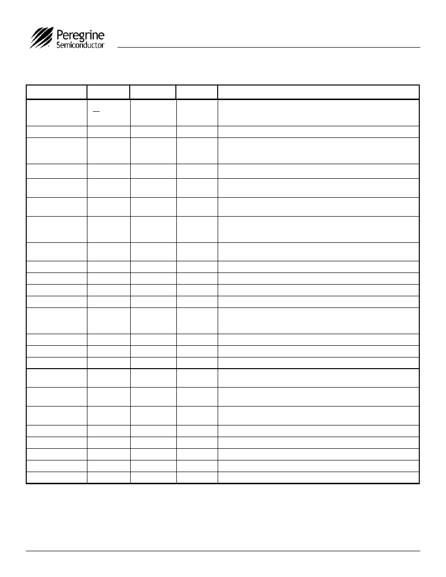
Fin
ALL
Input
Prescaler complementary input. A bypass capacitor should be placed as
close as possible to this pin and be connected in series with a 50
resistor
directly to the ground plane.
24
GND
ALL
Ground.
25
fp
ALL
Output
Monitor pin for main divider output. Switching activity can be disabled
through enhancement register programming or by floating or grounding VDD
pin 31.
26
VDD-fp
ALL
(Note 1)
VDD for fp. Can be left floating or connected to GND to disable the fp output.
27
Dout
Serial, Parallel
Output
Data Out. The MSEL signal and the raw prescaler output are available on
Dout through enhancement register programming.
28
VDD
ALL
(Note 1)
Power supply input. Input may range from 2.85 V to 3.15 V. Bypassing
recommended.
29
Cext
ALL
Output
Logical “NAND” of PD_
U and PD_D terminated through an on chip, 2 k
series resistor. Connecting Cext to an external capacitor will low pass filter
the input to the inverting amplifier used for driving LD.
30
VDD
ALL
(Note 1)
Power supply input. Input may range from 2.85 V to 3.15 V. Bypassing
recommended.
32
PD_
D
ALL
Output
PD_
D is pulse down when f
p leads fc.
33
PD_
U
ALL
PD_
U is pulse down when f
c leads fp.
35
VDD-fc
ALL
(Note 1)
VDD for fc can be left floating or connected to GND to disable the fc output.
36
fc
ALL
Output
Monitor pin for reference divider output. Switching activity can be disabled
through enhancement register programming or by floating or grounding VDD
pin 38.
31,37
GND
ALL
Ground.
38,39
GND
ALL
Ground.
40
fr
ALL
Input
Reference frequency input.
41
LD
ALL
Output
Lock detect and open drain logical inversion of CEXT. When the loop is in
lock, LD is high impedance, otherwise LD is a logic low (“0”).
42
Enh
Serial, Parallel
Input
Enhancement mode. When asserted low (“0”), enhancement register bits
are functional.
43
VDD
ALL
(Note 1)
Power supply input. Input may range from 2.85 V to 3.15 V. Bypassing
recommended.
44
R0
Direct
Input
R Counter bit0 (LSB).
45
R1
Direct
Input
R Counter bit1.
46
R2
Direct
Input
R Counter bit2.
47
R3
Direct
Input
R Counter bit3.
48
GND
ALL
(Note 1)
Ground.
34
NC
ALL
No connection.
Table 1. Pin Descriptions (continued)
Notes: 1. All VDD pins are connected by diodes and must be supplied with the same positive voltage level.
VDD-fp and VDD-fp are used to power the fp and fc outputs and can alternatively be left floating or connected to GND to disable the fp and fc outputs.
2. All digital input pins have 70 k
pull-down resistors to ground.
Pin No.
Pin Name
Interface Mode
Type
Description
Obsolete
Logo updated under non-rev change. Peregrine products are protected under one or more of the following U.S. Patents: http://patents.psemi.com
相关PDF资料 |
PDF描述 |
|---|---|
| 5P49EE602NLGI | IC CLOCK GENERATOR 24QFN |
| 5P49EE801NDGI | IC CLOCK GENERATOR 28QFN |
| 74ABT16240ADGG,518 | IC INVERTER QUAD 4-INPUT 48TSSOP |
| 74ABT16244ADGG,518 | IC BUFF DVR TRI-ST 16BIT 48TSSOP |
| 74ABT2240PW,118 | IC INVERTER DUAL 4-INPUT 20TSSOP |
相关代理商/技术参数 |
参数描述 |
|---|---|
| 33366 | 功能描述:CHUCK M DUTY KLESS 13MM 6JT JK13 制造商:apex tool group 系列:* 零件状态:在售 标准包装:1 |
| 333663-000 | 制造商:TE Connectivity 功能描述:44/0414-24-2CS1038 - Cable Rools/Shrink Tubing |
| 333-670A | 制造商:LG Corporation 功能描述:LEVERPOWER S/W (FK-670) |
| 3336796001 | 制造商:TE Connectivity 功能描述:RBK-ESS-CROSS-10.0-X-8MM - Bulk |
| 333682 | 制造商:n/a 功能描述:ERN1 S7K6B |
发布紧急采购,3分钟左右您将得到回复。