- 您现在的位置:买卖IC网 > PDF目录156551 > 37C669 (SMSC Corporation) DIODE SCHOTTKY SINGLE 25V 200mW 0.5V-vf 200mA-IFM 30mA-IF 2uA-IR SOD-323 3K/REEL PDF资料下载
参数资料
| 型号: | 37C669 |
| 厂商: | SMSC Corporation |
| 英文描述: | DIODE SCHOTTKY SINGLE 25V 200mW 0.5V-vf 200mA-IFM 30mA-IF 2uA-IR SOD-323 3K/REEL |
| 中文描述: | 电脑98/99顺从超级I / O软盘控制器与红外线支持 |
| 文件页数: | 36/164页 |
| 文件大小: | 621K |
| 代理商: | 37C669 |
第1页第2页第3页第4页第5页第6页第7页第8页第9页第10页第11页第12页第13页第14页第15页第16页第17页第18页第19页第20页第21页第22页第23页第24页第25页第26页第27页第28页第29页第30页第31页第32页第33页第34页第35页当前第36页第37页第38页第39页第40页第41页第42页第43页第44页第45页第46页第47页第48页第49页第50页第51页第52页第53页第54页第55页第56页第57页第58页第59页第60页第61页第62页第63页第64页第65页第66页第67页第68页第69页第70页第71页第72页第73页第74页第75页第76页第77页第78页第79页第80页第81页第82页第83页第84页第85页第86页第87页第88页第89页第90页第91页第92页第93页第94页第95页第96页第97页第98页第99页第100页第101页第102页第103页第104页第105页第106页第107页第108页第109页第110页第111页第112页第113页第114页第115页第116页第117页第118页第119页第120页第121页第122页第123页第124页第125页第126页第127页第128页第129页第130页第131页第132页第133页第134页第135页第136页第137页第138页第139页第140页第141页第142页第143页第144页第145页第146页第147页第148页第149页第150页第151页第152页第153页第154页第155页第156页第157页第158页第159页第160页第161页第162页第163页第164页
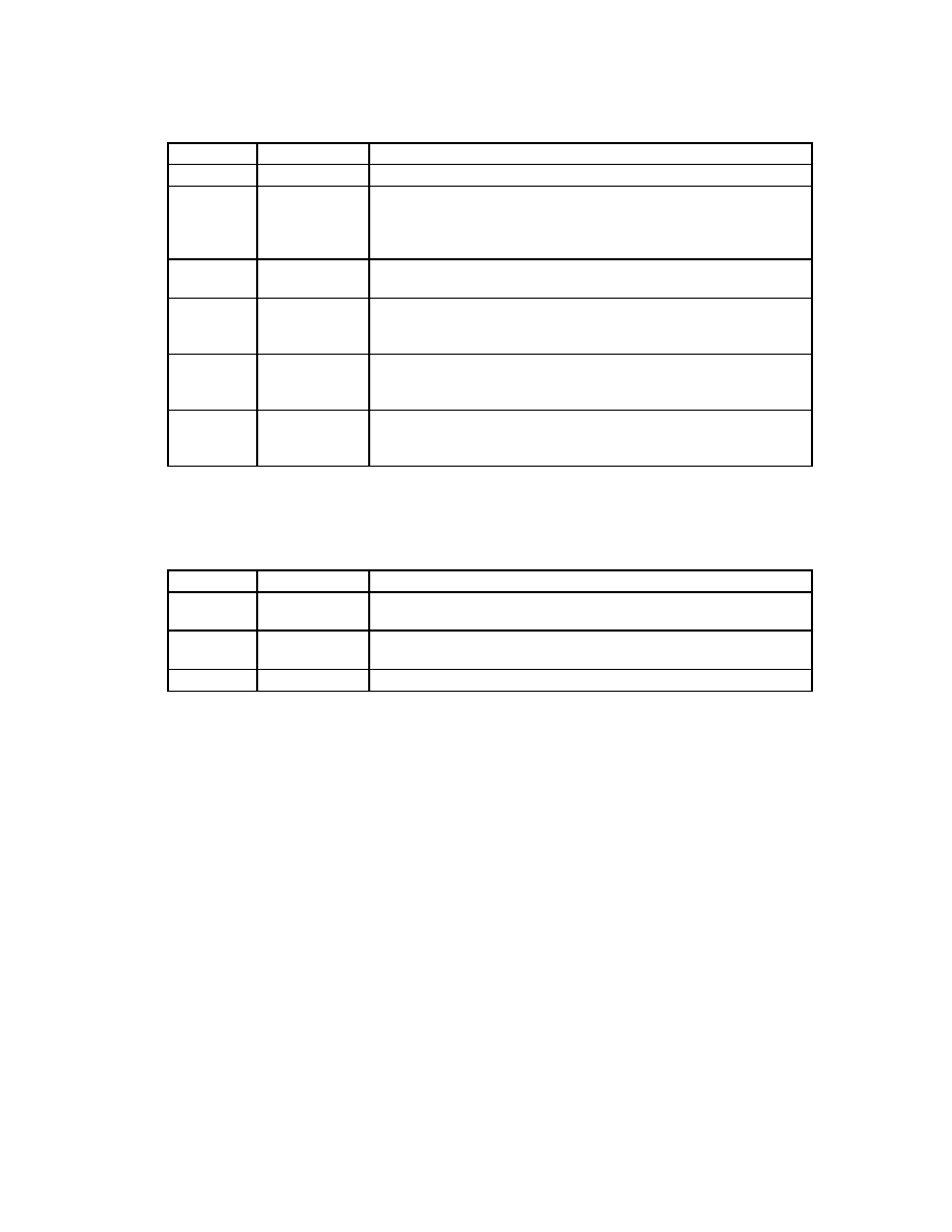
130
CR10
This
register
can
only be accessed in the
Configuration Mode and after the CSR has been
initialized to 10H.
The default value of this
register after power up is 00H.
Table 58 - CR10
BIT NO.
BIT NAME
DESCRIPTION
0 - 2
Reserved
Reserved - READ ONLY. A read returns a 0.
3
Pll Gain
This bit controls the gain of the frequency multiplying phase lock
loops. When a 0 (default) the gain is set to a value expected for 5
volt operation. When set to a 1 the gain is doubled to a value for
possible 3 volt operation.
4
Pll Stop
A 1 in this bit position stops the frequency multiplying phase lock
loops. A 0 (default) allows normal operation.
5
ACE_STOP
This bit when set to a 1 will inhibit the 24MHz clock to the divide by
12/13 that generates the UART clocks, and reset those dividers.
When at a 0 (default) these dividers and clocks are enabled.
6
PLL Clock
Control
This bit enables the PLL clock generator to run with either a
14.318MHz or 24MHz input clock. A 0 enables the 14.318MHz clock
(default), a 1 enables the 24MHz clock.
7
Infra Red Test
This bit enables the IR test mode. When this bit is set to a 1 the
serial data seen by UART RX and TX ports is output on SOUT. A 0
gives normal operation (default).
CR11
This
register
can
only be accessed in the
Configuration Mode and after the CSR has
been initialized to 11H. The default value of this
register after power up is 00H.
Table 59 - CR11
BIT NO.
BIT NAME
DESCRIPTION
0
IR Loop Back
When a 1 the IROUT is looped back internally to the IRIN input.
When a 0 (default) normal operation.
1
Test 10ms
This bit when a 1 tests the 10ms timeout of the FDC autopower down
mode. A 0 (default) allows normal operation.
2 - 7
Reserved
Reserved - READ ONLY. A read returns a 0.
相关PDF资料 |
PDF描述 |
|---|---|
| 37C672 | ENHANCED SUPER I/O CONTROLLER WITH FAST IR |
| 37C67X | ENHANCED SUPER I/O CONTROLLER WITH FAST IR |
| 37C957FR | ULTRA I/O CONTROLLER FOR PORTABLE APPLICATIONS |
| 37FMA1-ABW31N | SPECIAL SWITCH-PIEZO SWITCH, SPST, MOMENTARY, 0.2A, 24VDC, PANEL MOUNT-THREADED |
| 37FML1-BEW31N | SPECIAL SWITCH-PIEZO SWITCH, SPST, MOMENTARY, 0.2A, 24VDC, PANEL MOUNT-THREADED |
相关代理商/技术参数 |
参数描述 |
|---|---|
| 37C672 | 制造商:SMSC 制造商全称:SMSC 功能描述:ENHANCED SUPER I/O CONTROLLER WITH FAST IR |
| 37C67X | 制造商:SMSC 制造商全称:SMSC 功能描述:ENHANCED SUPER I/O CONTROLLER WITH FAST IR |
| 37C-6BH-5-5 | 制造商:Birtcher Products 功能描述: |
| 37C72U-185 | 制造商:White-Rodgers 功能描述: |
| 37C73U-170 | 制造商:White-Rodgers 功能描述: |
发布紧急采购,3分钟左右您将得到回复。