- 您现在的位置:买卖IC网 > PDF目录33810 > 48e30 (Holtek Semiconductor Inc.) 8-Bit I/O Type MCU (With EEPROM) PDF资料下载
参数资料
| 型号: | 48e30 |
| 厂商: | Holtek Semiconductor Inc. |
| 英文描述: | 8-Bit I/O Type MCU (With EEPROM) |
| 中文描述: | 8位I / O型微控制器(带EEPROM) |
| 文件页数: | 7/44页 |
| 文件大小: | 351K |
| 代理商: | 48E30 |
第1页第2页第3页第4页第5页第6页当前第7页第8页第9页第10页第11页第12页第13页第14页第15页第16页第17页第18页第19页第20页第21页第22页第23页第24页第25页第26页第27页第28页第29页第30页第31页第32页第33页第34页第35页第36页第37页第38页第39页第40页第41页第42页第43页第44页
HT48E30
Rev. 0.00
15
January 12, 2004
Preliminary
Input/Output Ports
There are 23 bidirectional input/output lines in the
microcontroller, labeled from PA to PC and PG, which
are mapped to the data memory of [12H], [14H], [16H]
and [1EH] respectively. All of these I/O ports can be
used for input and output operations. For input opera-
tion, these ports are non-latching, that is, the inputs
must be ready at the T2 rising edge of instruction
MOV
A,[m]
(m=12H, 14H, 16H or 1EH). For output operation,
all the data is latched and remains unchanged until the
output latch is rewritten.
Each I/O line has its own control register (PAC, PBC,
PCC, PGC) to control the input/output configuration.
With this control register, CMOS output or Schmitt trig-
ger input with or without pull-high resistor structures can
be reconfigured dynamically under software control. To
function as an input, the corresponding latch of the con-
trol register must write a
1. The input source also de-
pends on the control register. If the control register bit is
1, the input will read the pad state. If the control regis-
ter bit is
0, the contents of the latches will move to the
internal bus. The latter is possible in the
read-modify-write instruction.
For output function, CMOS is the only configuration.
These control registers are mapped to locations 13H,
15H, 17H and 1FH.
After a chip reset, these input/output lines remain at high
levels or floating state (depending on the pull-high op-
tions). Each bit of these input/output latches can be set
or cleared by
SET [m].i and CLR [m].i (m=12H, 14H,
16H or 1EH) instructions.
Some instructions first input data and then follow the
output operations. For example,
SET [m].i, CLR
[m].i
, CPL [m], CPLA [m] read the entire port states
into the CPU, execute the defined operations
(bit-operation), and then write the results back to the
latches or the accumulator.
Each line of port A has the capability of waking-up the de-
vice. The highest 7-bit of port G are not physically imple-
mented; on reading them a
0 is returned whereas writing
then results in no operation. See Application note.
There is a pull-high option available for all I/O lines (bit
option). Once the pull-high option of an I/O line is se-
lected, the I/O line has a pull-high resistor. Otherwise,
the pull-high resistor is absent. It should be noted that a
non-pull-high I/O line operating in input mode will cause
a floating state.
The PB0 and PB1 are pin-shared with BZ and BZ sig-
nals, respectively. If the BZ/BZ option is selected, the
output signal in output mode of PB0/PB1 will be the PFD
signal generated by timer/event counter 0 overflow sig-
nal. The input mode always remain in its original func-
tions. Once the BZ/BZ option is selected, the buzzer
output signals are controlled by the PB0 data register
only.
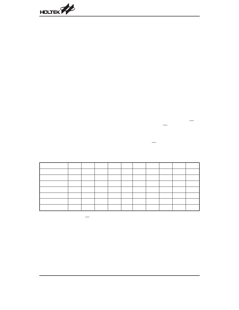
The I/O functions of PB0/PB1 are shown below.
PB0 I/O
I
OO
O
OOOOO
PB1 I/O
I
O
I
OOOOO
PB0 Mode
x
C
B
C
BBBB
PB1 Mode
x
C
x
C
B
PB0 Data
x
D
0
1
D0
0101
PB1 Data
x
D
x
D1
DD
x
PB0 Pad Status
I
D
0
B
D0
0B0B
PB1 Pad Status
I
D
I
D1
DD
0
B
Note:
I input, O output, D, D0,D1 data,
B buzzer option, BZ or BZ, x don’t care
C CMOS output
相关PDF资料 |
PDF描述 |
|---|---|
| 48L120D | STANDARD RECOVERY DIODES |
| 48L160D | STANDARD RECOVERY DIODES |
| 48LF120D | CAP 1500PF 50V CERAMIC MONO 5% |
| 48LF160D | STANDARD RECOVERY DIODES |
| 48LFR120D | STANDARD RECOVERY DIODES |
相关代理商/技术参数 |
参数描述 |
|---|---|
| 48-EM | 制造商:ITW Switches 功能描述:ELECTROMECHANICAL SWITCH KIT, Kit Contents:Miniature Sealed Electro-Mechanical P |
| 48ES | 制造商:VISUAL COMMUNICATIONS COMPANY LLC 功能描述:48ES /Custom Part |
| 48ESB | 功能描述:灯 Telephone Slide Base .04A .358M ANSI#5 RoHS:否 制造商:Chicago Miniature 灯类型:Incandescent 灯座类型:Wire Terminal 灯大小:T-1 3/4 颜色: 电压:14 V 工作电流: MSCP:0.3 MSCP 寿命:40000 hr 封装:Bulk |
| 48ESB- | 功能描述:LAMP T-2 TELEPHONE SLIDE 48V RoHS:是 类别:光电元件 >> 灯 - 白炽灯,氖灯 系列:- 标准包装:100 系列:- 颜色:透明 透镜样式/尺寸:圆形,带圆顶,5mm,T-1 3/4 引线型:小型凹槽 MSCP(平均球面烛光):0.3 额定电压:60V 其它名称:913.4005913.4005-ND |
| 48ESB | 制造商:PRIVATE LABEL 功能描述:Incandescent Filament Lamp, Voltage Rating:48V, Bulb Size:T-2, Lamp Ba Type:Slide |
发布紧急采购,3分钟左右您将得到回复。