- 您现在的位置:买卖IC网 > PDF目录67320 > 5962-0150601HXX (ANALOG DEVICES INC) DUAL 1-CH 14-BIT PROPRIETARY METHOD ADC, PARALLEL ACCESS, CQFP68 PDF资料下载
参数资料
| 型号: | 5962-0150601HXX |
| 厂商: | ANALOG DEVICES INC |
| 元件分类: | ADC |
| 英文描述: | DUAL 1-CH 14-BIT PROPRIETARY METHOD ADC, PARALLEL ACCESS, CQFP68 |
| 封装: | CERAMIC, LCC-68 |
| 文件页数: | 3/20页 |
| 文件大小: | 3511K |
| 代理商: | 5962-0150601HXX |
REV. A
AD13465
–11–
Power Supplies
Care should be taken when selecting a power source. Linear
supplies are strongly recommended. Switching supplies tend to
have radiated components that may be received by the AD13465.
Each of the power supply pins should be decoupled as closely to
the package as possible, using 0.1
F chip capacitors.
The AD13465 has separate digital and analog power supply pins.
The analog supplies are denoted AVCC and the digital supply
pins are denoted DVCC. AVCC and DVCC should be separate
power supplies. This is because the fast digital output swings
can couple switching current back into the analog supplies.
Note that AVCC must be held within +5% and –3% of 5 V. The
AD13465 is specified for DVCC = 3.3 V, since this is a common
supply for digital ASICs.
Output Loading
Care must be taken when designing the data receivers for the
AD13465. The digital outputs drive an internal series resistor
(e.g., 100
) followed by a gate like 75LCX574. To minimize
capacitive loading, there should be only one gate on each output pin.
An example of this is shown in the evaluation board schematic
shown in Figure 10. The digital outputs of the AD13465 have a
constant output slew rate of 1 V/ns. A typical CMOS gate combined
with a PCB trace will have a load of approximately 10 pF. Therefore,
as each bit switches, 10 mA (10 pF
× 1 V ÷ 1 ns) of dynamic current
per bit will flow in or out of the device. A full-scale transition
can cause up to 140 mA (14 bits
× 10 mA/bit) of transient
current through the output stages. These switching currents are
confined between ground and the DVCC pin. Standard TTL
gates should be avoided since they can appreciably add to the
dynamic switching currents of the AD13465. It should also be
noted that extra capacitive loading will increase output timing and
invalidate timing specifications. Digital output timing is guaranteed
with 10 pF loads.
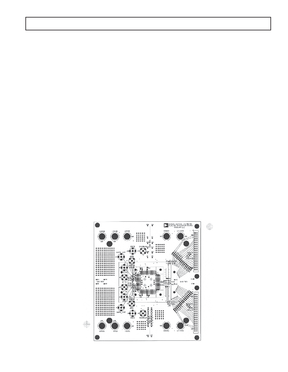
Figure 9. Evaluation Board Mechanical Layout
EVALUATION BOARD
The AD13465 evaluation board (Figure 9) is designed to
provide optimal performance for evaluation of the AD13465
analog-to-digital converter. The board encompasses everything
needed to ensure the highest level of performance for evaluating
the AD13465. The board requires an analog input signal, encode
clock, and power supply inputs. The clock is buffered on-board
to provide clocks for the latches. The digital outputs and out
clocks are available at the standard 40-pin connectors J1 and J2.
Power to the analog supply pins is connected via banana jacks.
The analog supply powers the associated components and
the analog section of the AD13465. The digital outputs of the
AD13465 are powered via banana jacks with 3.3 V. Contact the
factory if additional layout or applications assistance is required.
LAYOUT INFORMATION
The schematics of the evaluation board (Figures 10a–10
c) repre-
sent typical implementation of the AD13465. The pinout of the
AD13465 is very straightforward and facilitates ease of use and
the implementation of high frequency/high resolution design prac-
tices. It is recommended that high quality ceramic chip capacitors
be used to decouple each supply pin to ground directly at the
device. All capacitors can be standard high quality ceramic chip
capacitors.
Care should be taken when placing the digital output runs. Because
the digital outputs have such a high slew rate, the capacitive load-
ing on the digital outputs should be minimized. Circuit traces for
the digital outputs should be kept short and connect directly to the
receiving gate. Internal circuitry buffers the outputs of the ADC
through a resistor network to eliminate the need to externally
isolate the device from the receiving gate.
相关PDF资料 |
PDF描述 |
|---|---|
| 5962-0251002HXC | 1-OUTPUT 8 W DC-DC REG PWR SUPPLY MODULE |
| 5962-9213902HZC | 1-OUTPUT 12 W DC-DC REG PWR SUPPLY MODULE |
| 5962-9555902HXC | 2-OUTPUT 12 W DC-DC REG PWR SUPPLY MODULE |
| 5962-9214402HXC | 2-OUTPUT 15 W DC-DC REG PWR SUPPLY MODULE |
| 5962-9213902HXC | 1-OUTPUT 12 W DC-DC REG PWR SUPPLY MODULE |
相关代理商/技术参数 |
参数描述 |
|---|---|
| 5962015062963 | 制造商: 功能描述: 制造商:undefined 功能描述: |
| 5962015063140 | 制造商: 功能描述: 制造商:undefined 功能描述: |
| 5962015063593 | 制造商: 功能描述: 制造商:undefined 功能描述: |
| 5962015063695 | 制造商: 功能描述: 制造商:undefined 功能描述: |
| 5962015067534 | 制造商: 功能描述: 制造商:undefined 功能描述: |
发布紧急采购,3分钟左右您将得到回复。