- 您现在的位置:买卖IC网 > PDF目录122717 > 935262073551 (NXP SEMICONDUCTORS) 8-BIT, MROM, 25 MHz, MICROCONTROLLER, PQFP64 PDF资料下载
参数资料
| 型号: | 935262073551 |
| 厂商: | NXP SEMICONDUCTORS |
| 元件分类: | 微控制器/微处理器 |
| 英文描述: | 8-BIT, MROM, 25 MHz, MICROCONTROLLER, PQFP64 |
| 封装: | PLASTIC, QFP-64 |
| 文件页数: | 4/43页 |
| 文件大小: | 206K |
| 代理商: | 935262073551 |
第1页第2页第3页当前第4页第5页第6页第7页第8页第9页第10页第11页第12页第13页第14页第15页第16页第17页第18页第19页第20页第21页第22页第23页第24页第25页第26页第27页第28页第29页第30页第31页第32页第33页第34页第35页第36页第37页第38页第39页第40页第41页第42页第43页
2000 Feb 21
12
Philips Semiconductors
Product specication
Multiprotocol IC Card coupler
TDA8006
ISO 7816 security
The correct sequence during activation and deactivation of
the card is ensured by a specific sequencer clocked at a
frequency which is a division ratio of the internal oscillator.
Activation (bit CMDVCC within the ports extension register
HIGH) is only possible if the card is present (pin PRES
HIGH or LOW according to the mask option) and if the
supply voltage is correct (ALARM signal inactive).
The presence of the card is signalled to the controller by
the OFF bit (within the UART status register), generating
an interrupt, if enabled, when toggling.
During a session, the sequencer performs an automatic
emergency deactivation in the event of card take-off,
supply voltage drop or short circuit. The OFF bit goes
LOW, thereby warning the controller through the interrupt
line INT0 and the status register.
Peripheral interface (see Figs 5 and 6)
This block allows parallel communication with the four
peripherals (ISO 7816 UART, clock generator, on/off
sequencer and auxiliary RAM) through an 8-bit data bus,
6-bit address and control bus and one interrupt line to the
controller. The data bus consists of ports P40 (data bit 0)
to P47 (data bit 7). The address bus consists of ports AD0
(P12), AD1 (P13), AD2 (P14) and AD3 (P15). The control
lines are R/W (P16) and EN (P17). The interrupt line is
INT0.
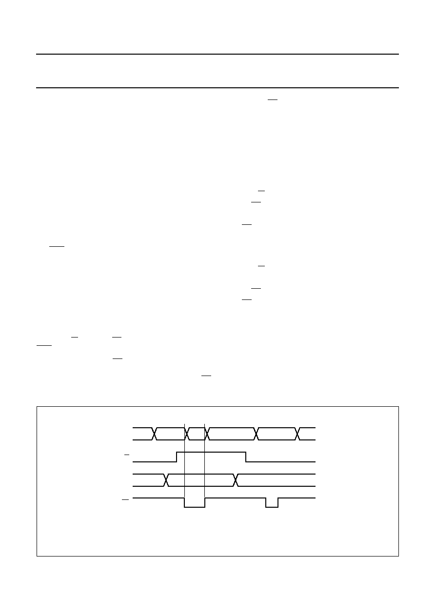
During a read operation, EN goes LOW allowing the
controller to read data on the bus. During a write operation,
the data should be present on the bus before asserting EN
LOW which allows the data to be written to the registers.
After resetting EN HIGH, the controller must release the
bus by setting port P4 HIGH again (the transition times on
port P4 are less than 500 ns).
The interrupt line is reset HIGH when reading out the
status register.
READ OPERATION
Set port P4 to FFH
Select the register with AD0, AD1, AD2, AD3
Assert R/W HIGH
Assert EN LOW; the data is available on data bus P4
Read the data on port P4
Set EN HIGH; the bus is set to high impedance.
WRITE OPERATION
Select the correct register with AD0, AD1, AD2, AD3
Assert R/W LOW
Write data to the data bus port P4
Assert EN LOW; the data is written to the register
Set EN HIGH
Set port P4 to FFH; the bus is set to high impedance.
Integrated precharges allow fast rising edges on port P4
when changing from read mode to write mode, thus
avoiding the need to trigger the active pull-ups on port P4.
handbook, full pagewidth
MGR229
P4
XX
FF
DATA
R/W
AD0 to AD3
X
AD
read data cycle
write data cycle
EN
DATA
Fig.5 Use of peripheral interface.
相关PDF资料 |
PDF描述 |
|---|---|
| 935263686557 | 6 CHANNEL(S), 200M bps, SERIAL COMM CONTROLLER, PQFP64 |
| 9173B-01CS08LF | 75 MHz, VIDEO CLOCK GENERATOR, PDSO8 |
| 9212AF-13LF-IN0 | 533.3 MHz, PROC SPECIFIC CLOCK GENERATOR, PDSO24 |
| 932S200BFLFT | 133 MHz, PROC SPECIFIC CLOCK GENERATOR, PDSO56 |
| 932S203AFLF | 133.3 MHz, PROC SPECIFIC CLOCK GENERATOR, PDSO56 |
相关代理商/技术参数 |
参数描述 |
|---|---|
| 935262217118 | 制造商:NXP Semiconductors 功能描述:Real Time Clock Serial 8-Pin SO T/R |
| 935264217557 | 制造商:NXP Semiconductors 功能描述:SUB ONLY IC |
| 935267356112 | 制造商:NXP Semiconductors 功能描述:IC TEA1507PN |
| 935268081112 | 制造商:NXP Semiconductors 功能描述:SUB ONLY IC |
| 935268721125 | 制造商:NXP Semiconductors 功能描述:Buffer/Line Driver 1-CH Non-Inverting 3-ST CMOS 5-Pin TSSOP T/R |
发布紧急采购,3分钟左右您将得到回复。