- 您现在的位置:买卖IC网 > PDF目录21914 > A1351KKTTN-T (Allegro Microsystems Inc)IC SENSOR HALL EFFECT 4-SIP PDF资料下载
参数资料
| 型号: | A1351KKTTN-T |
| 厂商: | Allegro Microsystems Inc |
| 文件页数: | 9/24页 |
| 文件大小: | 663K |
| 描述: | IC SENSOR HALL EFFECT 4-SIP |
| 产品培训模块: | Current Sensor |
| 产品变化通告: | Product Obsolescence 09/Nov/2011 |
| 标准包装: | 4,000 |
| 传感范围: | 0.055% ~ 0.095% DC/G |
| 类型: | 线性 - 单极,双极 |
| 电源电压: | 4.5 V ~ 5.5 V |
| 电流 - 电源: | 10mA |
| 电流 - 输出(最大): | 1mA |
| 输出类型: | 数字,推挽式 |
| 特点: | 高精度 |
| 工作温度: | -40°C ~ 125°C |
| 封装/外壳: | 4-SIP |
| 供应商设备封装: | 4-SIP |
| 包装: | 带卷 (TR) |
A1351
High Precision Linear Hall Effect Sensor IC
with a Push/Pull, Pulse Width Modulated Output
8
Allegro MicroSystems, Inc.
115 Northeast Cutoff
Worcester, Massachusetts 01615-0036 U.S.A.
1.508.853.5000; www.allegromicro.com
Characteristic Definitions
Power-On Time When the supply is ramped to its operating
voltage, the device requires a finite time to power its internal
components before supplying a valid PWM output duty cycle.
Power-On Time, t
PO
, is defined as: the time it takes for the output
voltage to settle within ?% D of its steady state value with no
applied magnetic field, after the power supply has reached its
minimum specified operating voltage, V
CC
(min).
Response Time The time interval between a) when the applied
magnetic field reaches 90% of its final value, and b) when the
device reaches 90% of its output corresponding to the applied
magnetic field.
Settling Time After Removal of Overload Magnetic Field The
pulse width modulated output, PWMOUT, of the Hall element
requires a finite time to recover from an overload magnetic field.
The amount of time, t
SETTLE
, the device takes to recover from
the overload is defined as: the time it takes for the quiescent Hall
output duty cycle, D
OUT(Q)
, to settle to within ?% D of its steady
state value after the overload field has fallen below 100 G. For
this specification the overload field should step from 5000 G to
0 G in less than 1ms.
Quiescent Voltage Output In the quiescent state (no significant
magnetic field: B = 0 G), the output duty cycle, D
(Q)
, equals a
specific programmed duty cycle throughout the entire operating
ranges of V
CC
and ambient temperature, T
A
.
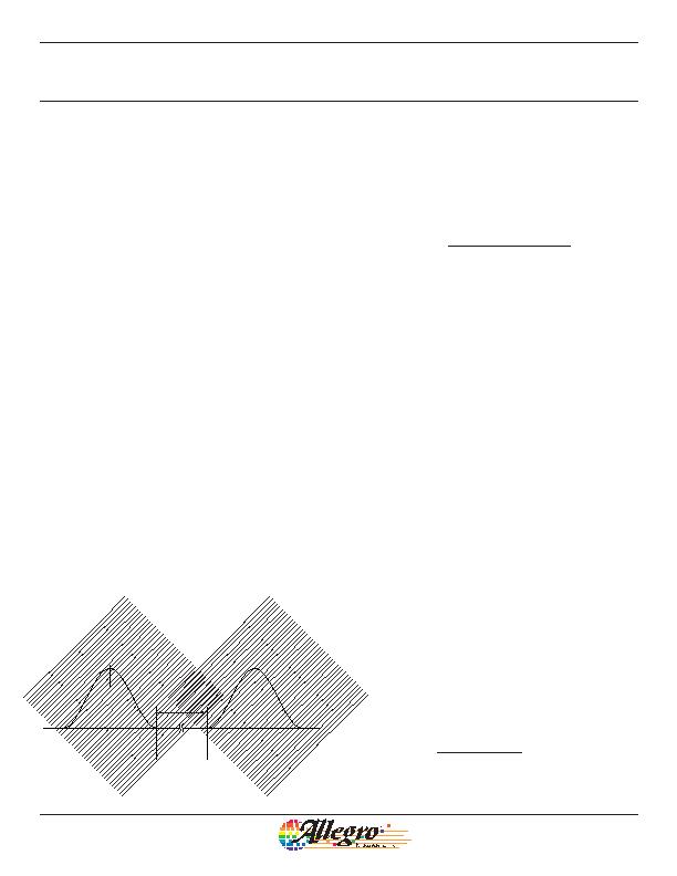
Guaranteed Quiescent Duty Cycle Output Range The quies-
cent duty cycle output, D
(Q)
, can be programmed around its nomi-
nal value of 50% D or 10% D, within the guaranteed quiescent
duty cycle range limits: D
(Q)
(min) and D
(Q)
(max). The available
guaranteed programming range for D
(Q)
falls within the distribu-
tions of the initial, D
(Q)init
, and the maximum programming code
for setting D
(Q)
, as shown in the following diagram.
D
(Q)
(max)
D
(Q)
(min)
D
(Q)init
(typ)
Guaranteed D
(Q)
Programming
Range
Max Code D
(Q)
Distribution
Initial D
(Q)
Distribution
Average Quiescent Voltage Output Step Size The average
quiescent duty cycle output step size for a single device is deter-
mined using the following calculation:
D
(Q)maxcode
D
(Q)init
2
n
1
Step
D(Q)
=
.
(1)
where:
n is the number of available programming bits in the trim range,
2
n
1 is the value of the maximum programming code in the
range, and
D
(Q)maxcode
is the quiescent duty cycle output at code 2
n
1.
Quiescent Duty Cycle Output Programming Resolution The
programming resolution for any device is half of its programming
step size. Therefore, the typical programming resolution will be:
Err
PGD(Q)
(typ)
=0.5 ?/SPAN> Step
D(Q)
(typ)
.
(2)
Quiescent Duty Cycle Output Drift Through Temperature
Range Due to internal component tolerances and thermal consid-
erations, the quiescent duty cycle output, D
(Q)
, may drift from its
nominal value over the operating ambient temperature, T
A
. For
purposes of specification, the Quiescent Duty Cycle Output Drift
Through Temperature Range, D
(Q)
(%D), is defined as:
D
(Q)
D
(Q)(TA)
D
(Q)(25癈)
=
.
(3)
D
(Q)
should be calculated using the actual measured values of
D
(Q)(TA)
and D
(Q)(25癈)
rather than programming target values.
Sensitivity The presence of a south polarity magnetic field,
perpendicular to the branded surface of the package face,
increases the output duty cycle from its quiescent value toward
the maximum duty cycle limit. The amount of the output duty
cycle increase is proportional to the magnitude of the magnetic
field applied. Conversely, the application of a north polarity
field decreases the output duty cycle from its quiescent value.
This proportionality is specified as the magnetic sensitivity, Sens
(%D/G), of the device, and it is defined for bipolar devices as:
D
(BPOS)
D
(BNEG)
BPOS BNEG
Sens
=
,
(4)
相关PDF资料 |
PDF描述 |
|---|---|
| 3864-48 | CORD DBL BANANA PLUG COILED 48" |
| DMN3029LFG-13 | MOSFET N-CH 30V 5.3A PWRDI333-8 |
| 2239-C-48 | MULTI-STACK BANANA PLUG RG58 48" |
| A1186LLHLT-T | IC SWITCH HALL EFFECT UNI SOT-23 |
| A1186EUA-T | IC SWITCH HALL EFFECT UNI 3-SIP |
相关代理商/技术参数 |
参数描述 |
|---|---|
| A1351LKTTN-T | 功能描述:IC SENSOR HALL EFFECT 4-SIP RoHS:是 类别:传感器,转换器 >> 磁性 - 霍尔效应,数字式开关,线性,罗盘 (IC) 系列:- 标准包装:1 系列:- 传感范围:20mT ~ 80mT 类型:旋转 电源电压:4.5 V ~ 5.5 V 电流 - 电源:15mA 电流 - 输出(最大):- 输出类型:数字式,PWM,8.5 位串行 特点:可编程 工作温度:-40°C ~ 150°C 封装/外壳:20-SSOP(0.209",5.30mm 宽) 供应商设备封装:20-SSOP 包装:Digi-Reel® 其它名称:AS5132-HSST-500DKR |
| A1352-035 | 制造商:AVX Corporation 功能描述: |
| A1352-037 | 制造商:AVX Corporation 功能描述: |
| A13532-43N | 制造商:Harris Corporation 功能描述: |
| A1354 | 制造商:ALLEGRO 制造商全称:Allegro MicroSystems 功能描述:High Precision 2-Wire Linear Hall Effect Sensor IC with Pulse Width Modulated Output |
发布紧急采购,3分钟左右您将得到回复。