- 您现在的位置:买卖IC网 > PDF目录164964 > A1361LKTTN-T MAGNETIC FIELD SENSOR-HALL EFFECT, 4.65-4.80V, RECTANGULAR, THROUGH HOLE MOUNT PDF资料下载
参数资料
| 型号: | A1361LKTTN-T |
| 元件分类: | 磁阻传感器 |
| 英文描述: | MAGNETIC FIELD SENSOR-HALL EFFECT, 4.65-4.80V, RECTANGULAR, THROUGH HOLE MOUNT |
| 封装: | LEAD FREE, PLASTIC, SIP-4 |
| 文件页数: | 21/25页 |
| 文件大小: | 615K |
| 代理商: | A1361LKTTN-T |
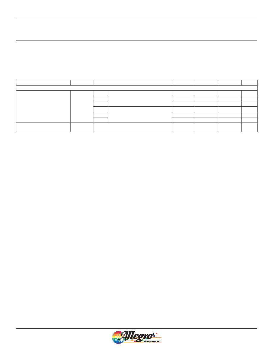
A1360, A1361,
and A1362
Characteristic
Symbol
Test Conditions
Min.
Typ.
Max.
Units
Drift Characteristics
Quiescent Voltage Output Drift
Through Temperature Range1
VOUT(Q)
A1360
VOUT(Q) = 2.5 V; Sens = Sens(min)
–20
–
20
mV
A1361
–20
–
20
mV
A1362
–60
–
60
mV
A1360
VOUT(Q) = 2.5 V; Sens = Sens(max)
– 35
–
35
mV
A1361
–50
–
50
mV
A1362
–160
–
160
mV
Sensitivity Drift Due to Package
Hysteresis1
SensPKG TA = 25°C, after temperature cycling
–
< ±1
–
%
1 See Characteristic Definitions section.
2 fC varies up to approximately ±20% over the full operating ambient temperature range, TA, and process.
3 VCLP voltages are production-tested, with the sole exception of the A1360 VCLP(HIGH), which is guaranteed by design (the low sensitivity and corresponding high
gauss levels required for testing A1360 VCLP(HIGH) make production testing impractical).
4 Noise is dependent on the sensitivity of the device and the filter capacitance. An 8 mV peak-to-peak noise floor exists that is independent of device sensitivity. This noise
floor attenuates proportionate to the filter capacitance (and device bandwidth).
5 Unit of measure (phase degrees) in reference to the magnetic input signal.
6 High-to-low transition of output voltage is a function of external load components and device sensitivity.
7 Raw device characteristic values before any programming.
8 VOUT(Q)UNIinit typically starts below the lower clamp voltage, VCLP(LOW). When programming the fine quiescent duty cycle for this parameter, several codes may need to be
addressed before VOUT(Q)UNI can be measured above VCLP(LOW).
9 Bits for selecting between VOUT(Q)UNI and VOUT(Q)BI programming ranges.
10 VOUT(Q) guaranteed by design.
11 VOUT(Q)(max) is the value available with all programming fuses blown (maximum programming code set). The VOUT(Q) range is the total range from VOUT(Q)init up to and
including VOUT(Q)(max). See Characteristic Definitions section. Quiescent Voltage Output may drift by an additional ±10 mV over the lifetime of this product.
12 Step size is larger than required, in order to provide for manufacturing spread. See Characteristic Definitions section.
13 Non-ideal behavior in the programming DAC can cause the step size at each significant bit rollover code to be greater than twice the maximum specified value of
StepVOUT(Q) or StepSENS.
14 Overall programming value accuracy. See Characteristic Definitions section.
15 Sens guaranteed by design.
16 Sens(max) is the value available with all programming fuses blown (maximum programming code set). Sens range is the total range from Sensinit up to and including
Sens(max). See Characteristic Definitions section. Sensitivity may drift by an additional ±2% over the lifetime of this product.
17 Programmed at 150°C and calculated relative to 25°C.
18 Linearity is only guaranteed for output voltage ranges of ±2 V from the quiescent output for bidirectional devices and +2 V from the quiescent output for unidirectional
devices. These linearity ranges are only valid within the operating output range of the device. The operating output range is confined to the region between the output clamps.
Linearity may shift by up to +/- 1 % over the lifetime of this product.
19 Symmetry error is only valid for bidirectional devices. Symmetry may shift by up to ±1% over the lifetime of this product.
20 Percent change from actual value at VCC = 5 V, for a given temperature, over the guaranteed supply voltage operating range.
21 Percent change from actual value at VCC = 5 V, TA = 25°C, over the guaranteed supply voltage operating range.
OPERATING CHARACTERISTICS (continued)
valid over full operating temperature range, TA; CBYPASS = 0.1 μF, VCC = 5 V, unless otherwise specied
Low-Noise Programmable Linear Hall Effect Sensor ICs with
Adjustable Bandwidth (50 kHz Maximum) and Analog Output
5
Allegro MicroSystems, Inc.
115 Northeast Cutoff
Worcester, Massachusetts 01615-0036 U.S.A.
1.508.853.5000; www.allegromicro.com
相关PDF资料 |
PDF描述 |
|---|---|
| A150N50X4A | 0 MHz - 2700 MHz 50 ohm RF/MICROWAVE TERMINATION |
| A15QS1-2 | FAST BLOW ELECTRIC FUSE, 1A, 150VAC, 150VDC, 100000A (IR), INLINE/HOLDER |
| A15QS10-2 | FAST BLOW ELECTRIC FUSE, 10A, 150VAC, 150VDC, 100000A (IR), INLINE/HOLDER |
| A15QS100-4TI | FAST BLOW ELECTRIC FUSE, 100A, 150VAC, 150VDC, 100000A (IR), INLINE/HOLDER |
| A15QS100-4 | FAST BLOW ELECTRIC FUSE, 100A, 150VAC, 150VDC, 100000A (IR), INLINE/HOLDER |
相关代理商/技术参数 |
参数描述 |
|---|---|
| A1362LKTTN-T | 功能描述:IC HALL EFFECT SENSOR LN 4-SIP RoHS:是 类别:传感器,转换器 >> 磁性 - 霍尔效应,数字式开关,线性,罗盘 (IC) 系列:- 标准包装:1 系列:- 传感范围:20mT ~ 80mT 类型:旋转 电源电压:4.5 V ~ 5.5 V 电流 - 电源:15mA 电流 - 输出(最大):- 输出类型:数字式,PWM,8.5 位串行 特点:可编程 工作温度:-40°C ~ 150°C 封装/外壳:20-SSOP(0.209",5.30mm 宽) 供应商设备封装:20-SSOP 包装:Digi-Reel® 其它名称:AS5132-HSST-500DKR |
| A1363LKTTN-10-T | 功能描述:IC HALL SENSOR 6.4-14MV/G 4SIP 制造商:allegro microsystems, llc 系列:- 包装:剪切带(CT) 零件状态:有效 类型:线性 技术:霍尔效应 轴:单路 感应范围:- 电压 - 电源:4.5 V ~ 5.5 V 电流 - 电源(最大值):15mA 电流 - 输出(最大值):10mA 输出类型:模拟电压 分辨率:- 带宽:120kHz 工作温度:-40°C ~ 150°C(TA) 特性:可编程,温度补偿 封装/外壳:4-SIP 模块 供应商器件封装:4-SIP 标准包装:1 |
| A1363LKTTN-1-T | 功能描述:IC HALL SENSOR 0.6-1.3MV/G 4SIP 制造商:allegro microsystems, llc 系列:- 包装:剪切带(CT) 零件状态:有效 类型:线性 技术:霍尔效应 轴:单路 感应范围:- 电压 - 电源:4.5 V ~ 5.5 V 电流 - 电源(最大值):15mA 电流 - 输出(最大值):10mA 输出类型:模拟电压 分辨率:- 带宽:120kHz 工作温度:-40°C ~ 150°C(TA) 特性:可编程,温度补偿 封装/外壳:4-SIP 模块 供应商器件封装:模块 标准包装:1 |
| A1363LKTTN-2-T | 功能描述:IC HALL SENSOR 1.3-2.9MV/G 4SIP 制造商:allegro microsystems, llc 系列:- 包装:剪切带(CT) 零件状态:有效 类型:线性 技术:霍尔效应 轴:单路 感应范围:- 电压 - 电源:4.5 V ~ 5.5 V 电流 - 电源(最大值):15mA 电流 - 输出(最大值):10mA 输出类型:模拟电压 分辨率:- 带宽:120kHz 工作温度:-40°C ~ 150°C(TA) 特性:可编程,温度补偿 封装/外壳:4-SIP 模块 供应商器件封装:4-SIP 标准包装:1 |
| A1363LKTTN-5-T | 功能描述:IC HALL SENSOR 2.9-6.4MV/G 4SIP 制造商:allegro microsystems, llc 系列:- 包装:剪切带(CT) 零件状态:有效 类型:线性 技术:霍尔效应 轴:单路 感应范围:- 电压 - 电源:4.5 V ~ 5.5 V 电流 - 电源(最大值):15mA 电流 - 输出(最大值):10mA 输出类型:模拟电压 分辨率:- 带宽:120kHz 工作温度:-40°C ~ 150°C(TA) 特性:可编程,温度补偿 封装/外壳:4-SIP 模块 供应商器件封装:4-SIP 标准包装:1 |
发布紧急采购,3分钟左右您将得到回复。