- 您现在的位置:买卖IC网 > PDF目录294789 > A40MX04-PLG44A FPGA, 6000 GATES, PQCC44 PDF资料下载
参数资料
| 型号: | A40MX04-PLG44A |
| 元件分类: | FPGA |
| 英文描述: | FPGA, 6000 GATES, PQCC44 |
| 封装: | PLASTIC, LCC-44 |
| 文件页数: | 29/76页 |
| 文件大小: | 429K |
| 代理商: | A40MX04-PLG44A |
第1页第2页第3页第4页第5页第6页第7页第8页第9页第10页第11页第12页第13页第14页第15页第16页第17页第18页第19页第20页第21页第22页第23页第24页第25页第26页第27页第28页当前第29页第30页第31页第32页第33页第34页第35页第36页第37页第38页第39页第40页第41页第42页第43页第44页第45页第46页第47页第48页第49页第50页第51页第52页第53页第54页第55页第56页第57页第58页第59页第60页第61页第62页第63页第64页第65页第66页第67页第68页第69页第70页第71页第72页第73页第74页第75页第76页
MX Automotive Family FPGAs
v2.0
1-29
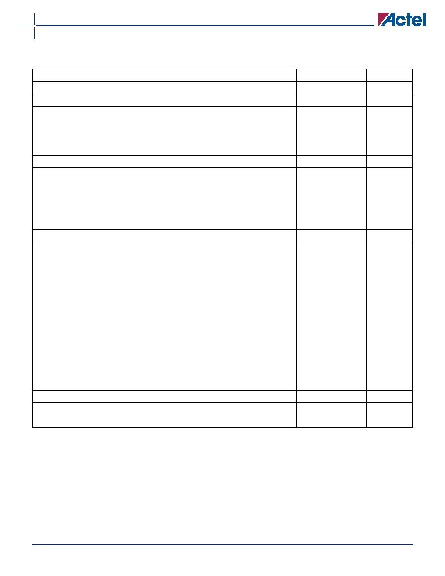
Table 1-7 A42MX09 Timing Characteristics (Nominal 5.0V Operation)
Worst-Case Automotive Conditions, VCC = 4.75V, TJ = 125°C
‘Std’ Speed
Parameter
Description
Min.
Max.
Units
Logic Module Propagation Delays1
tPD1
Single Module
2.1
ns
tCO
Sequential Clock-to-Q
2.2
ns
tGO
Latch G-to-Q
2.1
ns
tRS
Flip-Flop (Latch) Reset-to-Q
2.5
ns
Logic Module Predicted Routing Delays2
tRD1
FO=1 Routing Delay
1.2
ns
tRD2
FO=2 Routing Delay
1.7
ns
tRD3
FO=3 Routing Delay
2.0
ns
tRD4
FO=4 Routing Delay
2.4
ns
tRD8
FO=8 Routing Delay
4.0
ns
Logic Module Sequential Timing3, 4
tSUD
Flip-Flop (Latch) Data Input Set-Up
0.6
ns
tHD
Flip-Flop (Latch) Data Input Hold
0.0
ns
tSUENA
Flip-Flop (Latch) Enable Set-Up
0.7
ns
tHENA
Flip-Flop (Latch) Enable Hold
0.0
ns
tWCLKA
Flip-Flop (Latch) Clock Active Pulse Width
5.9
ns
tWASYN
Flip-Flop (Latch) Asynchronous Pulse Width
7.8
ns
tA
Flip-Flop Clock Input Period
6.0
ns
tINH
Input Buffer Latch Hold
0.0
ns
tINSU
Input Buffer Latch Set-Up
0.5
ns
tOUTH
Output Buffer Latch Hold
0.0
ns
tOUTSU
Output Buffer Latch Set-Up
0.5
ns
fMAX
Flip-Flop (Latch) Clock Frequency
229
MHz
Input Module Propagation Delays
tINYH
Pad-to-Y HIGH
1.9
ns
tINYL
Pad-to-Y LOW
1.4
ns
1. For dual-module macros, use tPD1 + tRD1 + tPDn, tCO + tRD1 + tPDn, or tPD1 + tRD1 + tSUD, whichever is appropriate.
2. Routing delays are for typical designs across worst-case operating conditions. These parameters should be used for estimating
device performance. Post-route timing analysis or simulation is required to determine actual performance.
3. Data applies to macros based on the S-module. Timing parameters for sequential macros constructed from C-modules can be
obtained from the Timer utility.
4. Set-up and hold timing parameters for the input buffer latch are defined with respect to the PAD and the D input. External setup/
hold timing parameters must account for delay from an external PAD signal to the G inputs. Delay from an external PAD signal to
the G input subtracts (adds) to the internal setup (hold) time.
5. Delays based on 35 pF loading.
相关PDF资料 |
PDF描述 |
|---|---|
| A40MX04-PLG68A | FPGA, 6000 GATES, PQCC68 |
| A42MX36-BG272A | FPGA, 54000 GATES, PBGA272 |
| A42MX36-BGG272A | FPGA, 54000 GATES, PBGA272 |
| A42MX36-CQ208A | FPGA, 54000 GATES, CQFP208 |
| A42MX36-CQ256A | FPGA, 54000 GATES, CQFP256 |
相关代理商/技术参数 |
参数描述 |
|---|---|
| A40MX04-PLG44I | 功能描述:IC FPGA MX SGL CHIP 6K 44-PLCC RoHS:是 类别:集成电路 (IC) >> 嵌入式 - FPGA(现场可编程门阵列) 系列:MX 标准包装:90 系列:ProASIC3 LAB/CLB数:- 逻辑元件/单元数:- RAM 位总计:36864 输入/输出数:157 门数:250000 电源电压:1.425 V ~ 1.575 V 安装类型:表面贴装 工作温度:-40°C ~ 125°C 封装/外壳:256-LBGA 供应商设备封装:256-FPBGA(17x17) |
| A40MX04-PLG44M | 制造商:Microsemi Corporation 功能描述:FPGA 6K GATES 547 CELLS 83MHZ/139MHZ 0.45UM 3.3V/5V 44PLCC - Rail/Tube 制造商:Microsemi Corporation 功能描述:IC FPGA 34 I/O 44PLCC |
| A40MX04-PLG68 | 功能描述:IC FPGA 69I/O 68PLCC RoHS:是 类别:集成电路 (IC) >> 嵌入式 - FPGA(现场可编程门阵列) 系列:MX 标准包装:24 系列:ECP2 LAB/CLB数:1500 逻辑元件/单元数:12000 RAM 位总计:226304 输入/输出数:131 门数:- 电源电压:1.14 V ~ 1.26 V 安装类型:表面贴装 工作温度:0°C ~ 85°C 封装/外壳:208-BFQFP 供应商设备封装:208-PQFP(28x28) |
| A40MX04-PLG68I | 功能描述:IC FPGA MX SGL CHIP 6K 68-PLCC RoHS:是 类别:集成电路 (IC) >> 嵌入式 - FPGA(现场可编程门阵列) 系列:MX 标准包装:90 系列:ProASIC3 LAB/CLB数:- 逻辑元件/单元数:- RAM 位总计:36864 输入/输出数:157 门数:250000 电源电压:1.425 V ~ 1.575 V 安装类型:表面贴装 工作温度:-40°C ~ 125°C 封装/外壳:256-LBGA 供应商设备封装:256-FPBGA(17x17) |
| A40MX04-PLG68M | 制造商:Microsemi Corporation 功能描述:FPGA 6K GATES 547 CELLS 83MHZ/139MHZ 0.45UM 3.3V/5V 68PLCC - Rail/Tube 制造商:Microsemi Corporation 功能描述:IC FPGA 57 I/O 68PLCC 制造商:Microsemi Corporation 功能描述:IC FPGA MX SGL CHIP 6K 68-PLCC |
发布紧急采购,3分钟左右您将得到回复。