- 您现在的位置:买卖IC网 > PDF目录364584 > A63L73321SERIES 128K X 32 Bit Synchronous High Speed SRAM with Burst Counter and Flow-through Data Output PDF资料下载
参数资料
| 型号: | A63L73321SERIES |
| 元件分类: | 通用总线功能 |
| 英文描述: | 128K X 32 Bit Synchronous High Speed SRAM with Burst Counter and Flow-through Data Output |
| 中文描述: | 128K的× 32位同步计数器高的Burst SRAM的速度和流量,通过数据输出 |
| 文件页数: | 11/17页 |
| 文件大小: | 270K |
| 代理商: | A63L73321SERIES |
A63L73321 Series
PRELIMINARY (June, 1999, Version 0.1)
10
AMIC Technology, Inc.
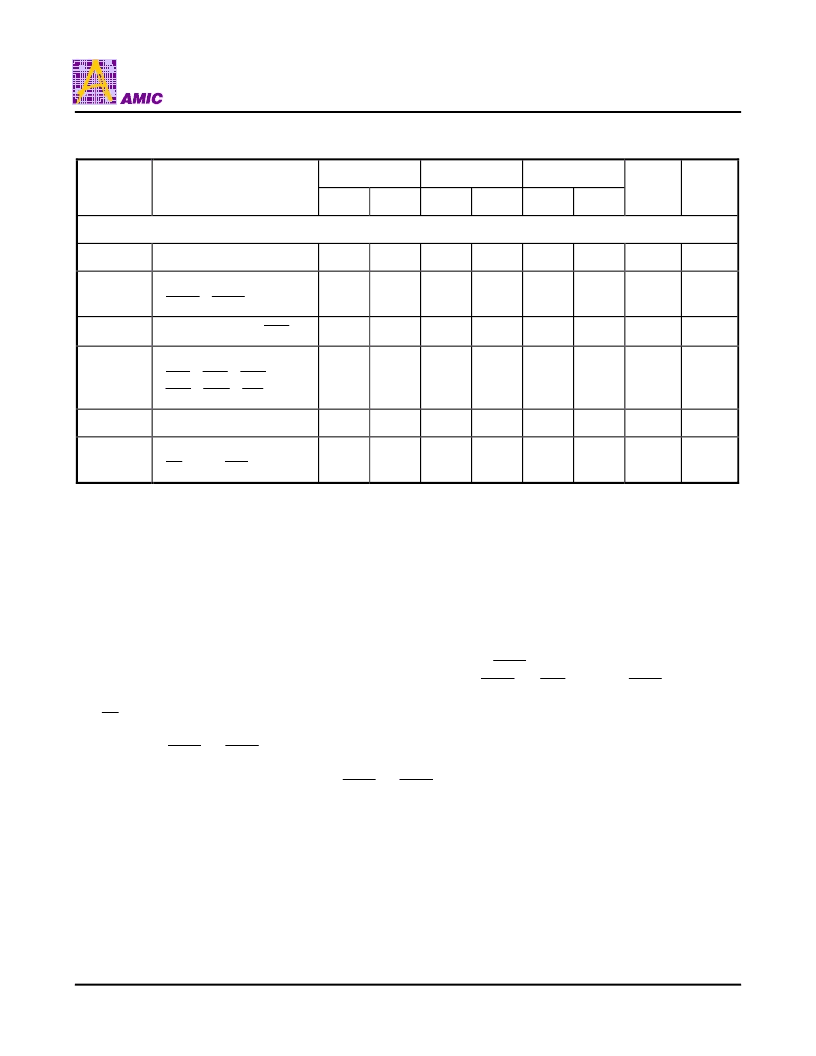
AC Characteristics (continued)
Symbol
Parameter
-9.5
-10
-12
Unit
Note
Min.
Max.
Min.
Max.
Min.
Max.
Hold Times
t
AH
Address
0.5
-
0.5
-
0.5
-
ns
7, 9
t
ADSH
Address Status
(
ADSC
,
ADSP
)
0.5
-
0.5
-
0.5
-
ns
7, 9
t
AAH
Address Advance (
ADV
)
0.5
-
0.5
-
0.5
-
ns
7, 9
t
WH
Write Signal
(
BW1
,
BW2
,
BW3
,
BW4
,
BWE
,
GW
)
0.5
-
0.5
-
0.5
-
ns
7, 9
t
DH
Data-in
0.5
-
0.5
-
0.5
-
ns
7, 9
t
CEH
Chip Enable
(
CE
, CE2,
CE2
)
0.5
-
0.5
-
0.5
-
ns
7, 9
Notes:
1.
2.
All voltages refer to GND.
Overshoot:
Undershoot: V
IH
≥
-0.7V for t
≤
t
KC
/2.
Power-up:
V
IH
≤
+3.6 and VCC
≤
3.1V
for t
≤
200ms
I
CC1
is given with no output current. I
CC1
increases with greater output loading and faster cycle times.
Test conditions assume the output loading shown in Figure 1, unless otherwise specified.
For output loading, C
L
= 5pF, as shown in Figure 2. Transition is measured
±
150mV from steady state voltage.
At any given temperature and voltage condition, t
KQHZ
is less than t
KQLZ
and t
OEHZ
is less than t
QELZ
.
A WRITE cycle is defined by at least one Byte Write enable LOW and
ADSP
HIGH for the required setup and hold
times. A READ cycle is defined by all byte write enables HIGH and (
ADSC
or
ADV
LOW) or
ADSP
LOW for the
required setup and hold times.
OE
has no effect when a Byte Write enable is sampled LOW.
This is a synchronous device. All addresses must meet the specified setup and hold times for all rising edges of CLK
when either
ADSP
or
ADSC
is LOW and the chip is enabled. All other synchronous inputs must meet the setup and
hold times with stable logic levels for all rising edges of clock (CLK) when the chip is enabled. Chip enable must be
valid at each rising edge of CLK when either
ADSP
or
ADSC
is LOW to remain enabled.
10. The load used for V
OH
, V
OL
testing is shown in Figure 2. AC load current is higher than the given DC values.
AC I/O curves are available upon request.
11. "Device Deselected" means device is in POWER-DOWN mode, as defined in the truth table. "Device Selected" means
device is active (not in POWER-DOWN mode).
12. MODE pin has an internal pulled-up, and ZZ pin has an internal pulled-down. All of then exhibit an input leakage
current of 10
μ
A.
13. Snooze (ZZ) input is recommended that users plan for four clock cycles to go into SLEEP mode and four clocks to
emerge from SLEEP mode to ensure no data is lost.
V
IH
≤
+4.6V for t
≤
t
KC
/2.
3.
4.
5.
6.
7.
8.
9.
相关PDF资料 |
PDF描述 |
|---|---|
| A6402 | Telecomm/Datacomm |
| a6402 | Universal Asynchronous Receiver/Transmitter(通用异步接收/传送器) |
| A65-1 | Analog IC |
| A655NV400C5 | Interface IC |
| 697NV400C5 | Microprocessor Supervisory Circuits |
相关代理商/技术参数 |
参数描述 |
|---|---|
| A63L7332E-42 | 制造商:AMICC 制造商全称:AMIC Technology 功能描述:128K X 32 Bit Synchronous High Speed SRAM with Burst Counter and Pipelined Data Output |
| A63L7332E-45 | 制造商:AMICC 制造商全称:AMIC Technology 功能描述:128K X 32 Bit Synchronous High Speed SRAM with Burst Counter and Pipelined Data Output |
| A63L7332E-5 | 制造商:AMICC 制造商全称:AMIC Technology 功能描述:128K X 32 Bit Synchronous High Speed SRAM with Burst Counter and Pipelined Data Output |
| A63L7332SERIES | 制造商:AMICC 制造商全称:AMIC Technology 功能描述:128K X 32 Bit Synchronous High Speed SRAM with Burst Counter and Pipelined Data Output |
| A63L7336 | 制造商:AMICC 制造商全称:AMIC Technology 功能描述:128K X 36 Bit Synchronous High Speed SRAM with Burst Counter and Pipelined Data Output |
发布紧急采购,3分钟左右您将得到回复。