参数资料
| 型号: | AD1877JRZ-RL |
| 厂商: | Analog Devices Inc |
| 文件页数: | 3/20页 |
| 文件大小: | 0K |
| 描述: | IC ADC STEREO 16BIT 28-SOIC |
| 标准包装: | 1,000 |
| 位数: | 16 |
| 采样率(每秒): | 45k |
| 数据接口: | 串行 |
| 转换器数目: | 2 |
| 功率耗散(最大): | 315mW |
| 电压电源: | 模拟和数字 |
| 工作温度: | 0°C ~ 70°C |
| 安装类型: | 表面贴装 |
| 封装/外壳: | 28-SOIC(0.295",7.50mm 宽) |
| 供应商设备封装: | 28-SOIC W |
| 包装: | 带卷 (TR) |
| 输入数目和类型: | 2 个单端,单极 |
AD1877
REV. A
–11–
Two modes deserve special discussion. The first special mode,
“Slave Mode, Data Position Controlled by WCLK Input” (S/M
= HI, RLJUST = HI, MSBDLY = LO), shown in Figure 8, is
the only mode in which WCLK is an input. The 16-bit output
data words can be placed at user-defined locations within 32-bit
fields. The MSB will appear in the BCLK period after WCLK is
detected HI by the BCLK sampling edge. If WCLK is HI dur-
ing the first BCLK of the 32-bit field (if WCLK is tied HI for
example), then the MSB of the output word will be valid on the
sampling edge of the second BCLK. The effect is to delay the
MSB for one bit clock cycle into the field, making the output
data compatible at the data format level with the I
2S data for-
mat. Note that the relative placement of the WCLK input can
vary from 32-bit field to 32-bit field, even within the same
64-bit frame. For example, within a single 64-bit frame, the left
word could be right justified (by pulsing WCLK HI on the 16th
BCLK) and the right word could be in an I
2S-compatible data
format (by having WCLK HI at the beginning of the second field).
In the second special mode “Master Mode, Right-Justified with
MSB Delay, WCLK Pulsed in 17th Cycle” (S/M = LO,
RLJUST = HI, MSBDLY = LO), shown in Figure 12, WCLK
is an output and is pulsed for one cycle by the AD1877. The
MSB is valid on the 18th BCLK sampling edge, and the LSB
extends into the first BCLK period of the next 32-bit field.
Timing Parameters
For master modes, a BCLK transmitting edge (labeled “XMIT”)
will be delayed from a CLKIN rising edge by tDLYCKB, as shown
in Figure 17. A LRCK transition will be delayed from a BCLK
transmitting edge by tDLYBLR. A WCLK rising edge will be
delayed from a BCLK transmitting edge by tDLYBWR, and a WCLK
falling edge will be delayed from a BCLK transmitting edge by
tDLYBWF. The DATA and TAG outputs will be delayed from a
transmitting edge of BCLK by tDLYDT.
For slave modes, an LRCK transition must be setup to a BCLK
sampling edge (labeled “SAMPLE”) by tSETLRBS. The DATA
and TAG outputs will be delayed from an LRCK transition by
tDLYLRDT, and DATA and TAG outputs will be delayed from
BCLK transmitting edge by tDLYBDT. For “Slave Mode, Data
Position Controlled by WCLK Input,” WCLK must be setup to
a BCLK sampling edge by tSETWBS.
For both master and slave modes, BCLK must have a minimum
LO pulsewidth of tBPWL, and a minimum HI pulsewidth of tBPWH.
The AD1877 CLKIN and RESET timing is shown in Figure
19. CLKIN must have a minimum LO pulsewidth of tCPWL, and
a minimum HI pulse width of tCPWH. The minimum period of
CLKIN is given by tCLKIN. RESET must have a minimum LO
pulsewidth of tRPWL. Note that there are no setup or hold time
requirements for RESET.
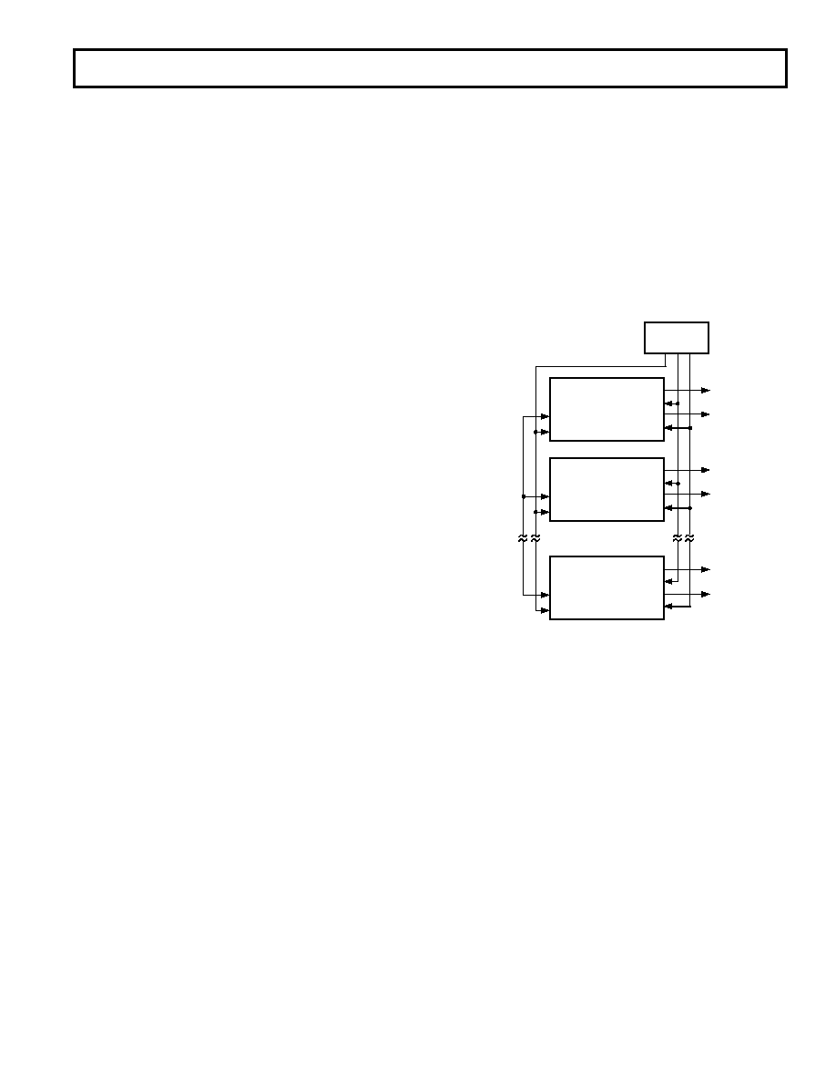
Synchronizing Multiple AD1877s
Multiple AD1877s can be synchronized by making all the
AD1877s serial port slaves. This option is illustrated in
Figure 6. See the “Reset, Autocalibration and Power Down”
section above for additional information.
#1 AD1877
SLAVE MODE
CLKIN
DATA
BCLK
WCLK
L
RCK
CLOCK
SOURCE
#2 AD1877
SLAVE MODE
CLKIN
DATA
BCLK
WCLK
L
RCK
#N AD1877
SLAVE MODE
CLKIN
DATA
BCLK
WCLK
L
RCK
RESET
Figure 6. Synchronizing Multiple AD1877s
相关PDF资料 |
PDF描述 |
|---|---|
| AD1974YSTZ-RL | IC CODEC 4CH ADC W/PLL 48-LQFP |
| AD2S99BP | IC OSC SINUSOIDAL 20KHZ 20-PLCC |
| AD5310BRM | IC DAC 10BIT R-R W/BUFF 8-MSOP |
| AD5341BRUZ | IC DAC 12BIT SNGL VOUT 20TSSOP |
| AD5344BRU | IC DAC 12BIT QUAD VOUT 28-TSSOP |
相关代理商/技术参数 |
参数描述 |
|---|---|
| AD1878 | 制造商:AD 制造商全称:Analog Devices 功能描述:High Performance 16-/18-Bit Stereo ADCs |
| AD1878JD | 制造商:AD 制造商全称:Analog Devices 功能描述:High Performance 16-/18-Bit Stereo ADCs |
| AD1879 | 制造商:AD 制造商全称:Analog Devices 功能描述:High Performance 16-/18-Bit Stereo ADCs |
| AD1879JD | 制造商:Rochester Electronics LLC 功能描述:- Bulk |
发布紧急采购,3分钟左右您将得到回复。