- 您现在的位置:买卖IC网 > PDF目录9287 > AD5263BRUZ50-REEL7 (Analog Devices Inc)IC POT DGTL 50K 256POS 24TSSOP PDF资料下载
参数资料
| 型号: | AD5263BRUZ50-REEL7 |
| 厂商: | Analog Devices Inc |
| 文件页数: | 10/28页 |
| 文件大小: | 0K |
| 描述: | IC POT DGTL 50K 256POS 24TSSOP |
| 标准包装: | 1,000 |
| 接片: | 256 |
| 电阻(欧姆): | 50k |
| 电路数: | 4 |
| 温度系数: | 标准值 30 ppm/°C |
| 存储器类型: | 易失 |
| 接口: | I²C,SPI(芯片选择,设备位址) |
| 电源电压: | 2.7 V ~ 5.5 V,5 V ~ 15 V |
| 工作温度: | -40°C ~ 125°C |
| 安装类型: | 表面贴装 |
| 封装/外壳: | 24-TSSOP(0.173",4.40mm 宽) |
| 供应商设备封装: | 24-TSSOP |
| 包装: | 带卷 (TR) |
第1页第2页第3页第4页第5页第6页第7页第8页第9页当前第10页第11页第12页第13页第14页第15页第16页第17页第18页第19页第20页第21页第22页第23页第24页第25页第26页第27页第28页
AD5263
Data Sheet
Rev. F | Page 18 of 28
The typical distribution of the end-to-end resistance RAB from
channel to channel matches within ±1%. Device-to-device
matching is process-lot dependent, and it is possible to have
±30% variation. Because the resistance element is processed in
thin film technology, the change in RAB with temperature has a
very low temperature coefficient of 30 ppm/°C.
PROGRAMMING THE POTENTIOMETER DIVIDER
VOLTAGE OUTPUT OPERATION
The digital potentiometer easily generates a voltage divider at
wiper-to-B and wiper-to-A proportional to the input voltage from
Terminal A and Terminal B. Unlike the polarity from VDD to VSS,
which must be positive, the voltage across A to B, W to A, and
W to B can be at either polarity, if VSS is powered by a negative
supply.
If the effect of the wiper resistance for approximation is ignored,
connecting the A terminal to 5 V and the B terminal to ground
produces an output voltage from the wiper to B, starting at 0 V
up to 1 LSB below 5 V. Each LSB step of voltage is equal to the
voltage applied across Terminal A to Terminal B divided by the
256 positions of the potentiometer divider. Because the AD5263
can be powered by dual supplies, the general equation defining
the output voltage VW with respect to ground for any valid input
voltages applied to Terminal A and Terminal B is
B
A
W
V
D
V
D
V
256
)
(
+
=
(3)
Operation of the digital potentiometer in the divider mode
results in a more accurate operation over temperature. Unlike
the rheostat mode, the output voltage is dependent mainly on
the ratio of the internal resistances RWA and RWB, and not their
absolute values; therefore, the temperature drift reduces to
5 ppm/°C.
PIN-SELECTABLE DIGITAL INTERFACE
The AD5263 provides the flexibility of a selectable interface.
When the digital interface select (DIS) pin is tied low, the SPI
mode is engaged. When the DIS pin is tied high to the VL
supply, the I2C mode is engaged.
SPI-COMPATIBLE 3-WIRE SERIAL BUS (DIS = 0)
The AD5263 contains a 3-wire SPI-compatible digital interface
(SDI, CS, and CLK). The 10-bit serial word must be loaded with
address bits A1 and A0, followed by the data byte, MSB first. The
format of the word is shown in the Serial Data-Word Format
section and bit map.
The positive-edge sensitive CLK input requires clean transitions
to avoid clocking incorrect data into the serial input register.
Standard logic families work well. If mechanical switches are
used for product evaluation, they should be debounced by a
flip-flop or other suitable means. When CS is low, the clock
loads data into the serial register on each positive clock edge
(see Figure 40).
Table 7. AD5263 Address Decode Table
A1
A0
Latch Loaded
0
RDAC 1
0
1
RDAC 2
1
0
RDAC 3
1
RDAC 4
The data setup and data hold times in the specification table
determine the valid timing requirements. The AD5263 uses a
10-bit serial input data register word that is transferred to the
internal RDAC register when the CS line returns to logic high.
Note that only the last 10 bits that are clocked into the register
are latched into the decoder. As CS goes high, it activates the
address decoder and updates the corresponding channel
according to Table 7.
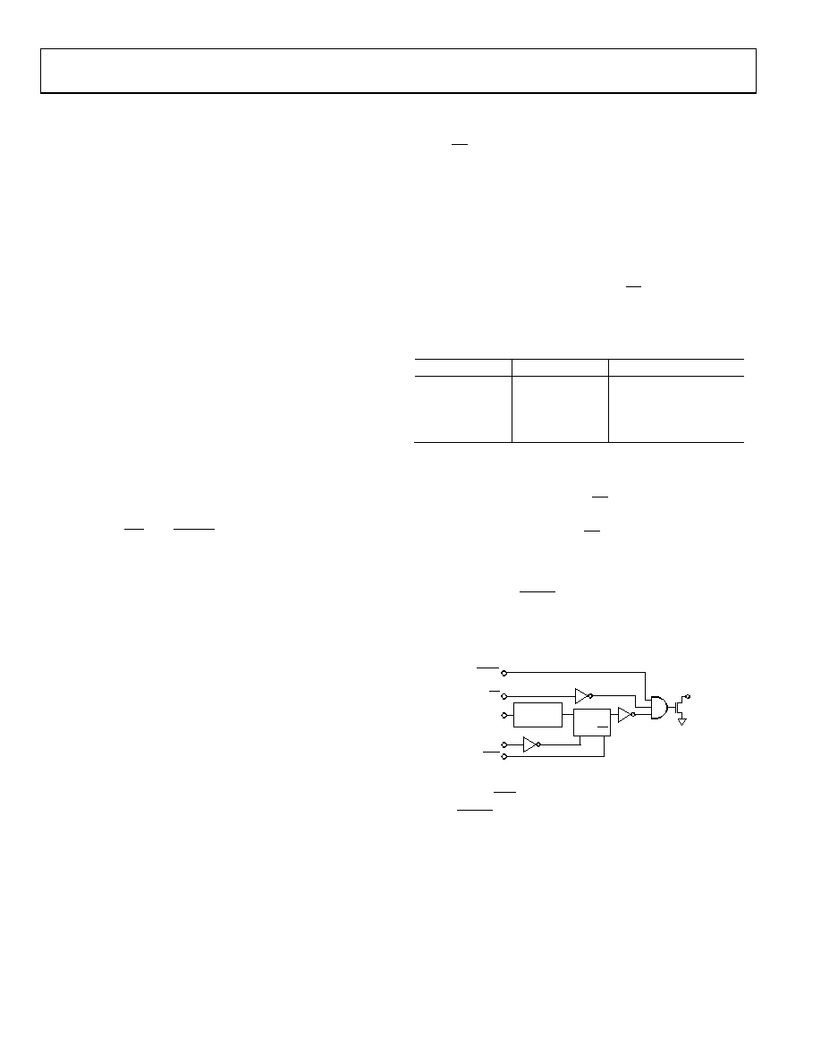
During shutdown (SHDN), the serial data output (SDO) pin is
forced to logic high in order to avoid power dissipation in the
external pull-up resistor. For an equivalent SDO output circuit
schematic, see Figure 46.
03142-
045
SERIAL
REGISTER
CS
SDI
CLK
SHDN
RES
RS
CK
SDO
D
Q
Figure 46. Detailed SDO Output Schematic of the AD5263
During reset (RES), the wiper is set to midscale. Note that
unlike SHDN, when the part is taken out of reset, the wiper
remains at midscale and does not revert to its pre-reset setting.
相关PDF资料 |
PDF描述 |
|---|---|
| DS1100Z-50+ | IC DELAY LINE 5TAP 50NS 8-SOIC |
| VE-272-MX-B1 | CONVERTER MOD DC/DC 15V 75W |
| MS27484T16A42PA | CONN PLUG 42POS STRAIGHT W/PINS |
| VI-B6H-IU-F4 | CONVERTER MOD DC/DC 52V 200W |
| VI-B4Z-MX-F4 | CONVERTER MOD DC/DC 2V 30W |
相关代理商/技术参数 |
参数描述 |
|---|---|
| AD5263EVAL | 制造商:Analog Devices 功能描述:Evaluation Board For Digital Potentiometer, Quad, 15V, 256-Position, Digital Potentiometer 制造商:Analog Devices 功能描述:AD5263 EVAL BOARD - Bulk |
| AD52651A | 制造商:ESMT 制造商全称:Elite Semiconductor Memory Technology Inc. 功能描述:2.5W/CH Stereo Filter-less Class-D Audio Amplifier with Headphone Driver |
| AD5266 | 制造商:ESMT 制造商全称:Elite Semiconductor Memory Technology Inc. 功能描述:16V STEREO CLASS-D AUDIO POWER AMPLIFIER with STEREO HEADPHONE |
| AD526A | 制造商:AD 制造商全称:Analog Devices 功能描述:Software Programmable Gain Amplifier |
| AD526AD | 功能描述:IC AMP PGA 10MA 16CDIP RoHS:否 类别:集成电路 (IC) >> Linear - Amplifiers - Instrumentation 系列:- 标准包装:2,500 系列:Excalibur™ 放大器类型:J-FET 电路数:1 输出类型:- 转换速率:45 V/µs 增益带宽积:10MHz -3db带宽:- 电流 - 输入偏压:20pA 电压 - 输入偏移:490µV 电流 - 电源:1.7mA 电流 - 输出 / 通道:48mA 电压 - 电源,单路/双路(±):4.5 V ~ 38 V,±2.25 V ~ 19 V 工作温度:-40°C ~ 85°C 安装类型:表面贴装 封装/外壳:8-SOIC(0.154",3.90mm 宽) 供应商设备封装:8-SOIC 包装:带卷 (TR) |
发布紧急采购,3分钟左右您将得到回复。