参数资料
| 型号: | AD5363BCPZ |
| 厂商: | Analog Devices Inc |
| 文件页数: | 11/29页 |
| 文件大小: | 0K |
| 描述: | IC DAC 14BIT 8CH SERIAL 56-LFCSP |
| 产品培训模块: | Data Converter Fundamentals DAC Architectures |
| 标准包装: | 1 |
| 设置时间: | 20µs |
| 位数: | 14 |
| 数据接口: | 串行 |
| 转换器数目: | 8 |
| 电压电源: | 双 ± |
| 功率耗散(最大): | 209mW |
| 工作温度: | -40°C ~ 85°C |
| 安装类型: | 表面贴装 |
| 封装/外壳: | 56-VFQFN 裸露焊盘,CSP |
| 供应商设备封装: | 56-LFCSP-VQ(8x8) |
| 包装: | 托盘 |
| 输出数目和类型: | 8 电压,单极;8 电压,双极 |
| 采样率(每秒): | * |
| 配用: | EVAL-AD5363EBZ-ND - BOARD EVALUATION FOR AD5363 |
第1页第2页第3页第4页第5页第6页第7页第8页第9页第10页当前第11页第12页第13页第14页第15页第16页第17页第18页第19页第20页第21页第22页第23页第24页第25页第26页第27页第28页第29页
AD5362/AD5363
Rev. A | Page 18 of 28
OUTPUT AMPLIFIER
Because the output amplifiers can swing to 1.4 V below the
positive supply and 1.4 V above the negative supply, this limits
how much the output can be offset for a given reference voltage.
For example, it is not possible to have a unipolar output range
of 20 V, because the maximum supply voltage is ±16.5 V.
CLR
DAC
CHANNEL
OFFSET
DAC
OUTPUT
R6
10k
R2
20k
S3
S2
S1
R4
60k
R3
20k
SIGGNDx
R5
60k
R1
20k
05
76
2-
0
22
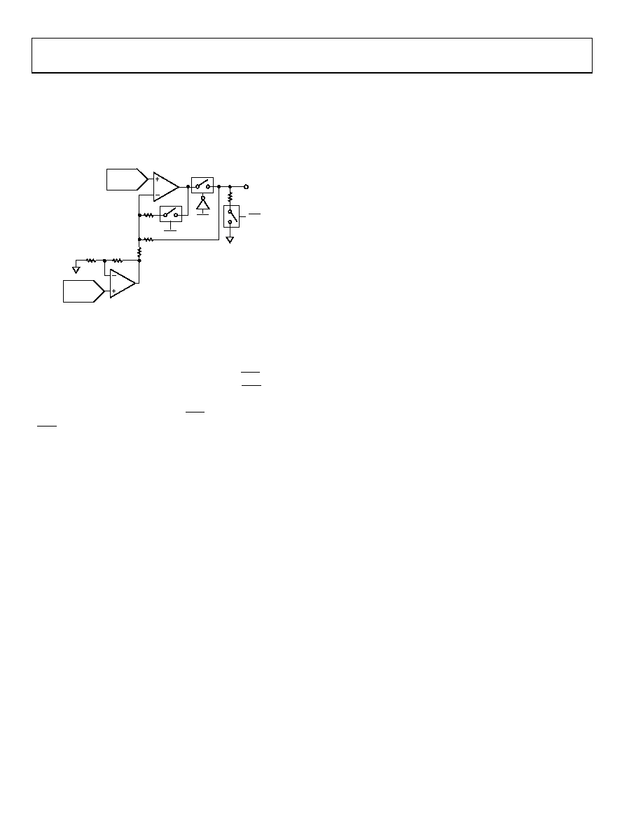
Figure 23. Output Amplifier and Offset DAC
Figure 23 shows details of a DAC output amplifier and its connec-
tions to the offset DAC. On power-up, S1 is open, disconnecting
the amplifier from the output. S3 is closed, so the output is pulled
to SIGGNDx (R1 and R2 are greater than R6). S2 is also closed to
prevent the output amplifier from being open-loop. If CLR is low at
power-up, the output remains in this condition until CLR is taken
high. The DAC registers can be programmed, and the outputs
assume the programmed values when CLR is taken high. Even if
CLR is high at power-up, the output remains in this condition
until VDD > 6 V and VSS < 4 V and the initialization sequence has
finished. The outputs then go to their power-on default value.
TRANSFER FUNCTION
The output voltage of a DAC in the AD5362/AD5363 is depen-
dent on the value in the input register, the value of the M and C
registers, and the value in the offset DAC.
AD5362 Transfer Function
The input code is the value in the X1A or X1B register that is
applied to the DAC (X1A, X1B default code = 32,768).
DAC_CODE = INPUT_CODE × (M + 1)/216 + C 215
where:
M = code in gain register default code = 216 – 1.
C = code in offset register default code = 215.
The DAC output voltage is calculated as follows:
VOUT = 4 × VREF × (DAC_CODE (OFFSET_CODE ×
4))/216 + VSIGGND
where:
DAC_CODE should be within the range of 0 to 65,535.
For 12 V span, VREF = 3.0 V.
For 20 V span, VREF = 5.0 V.
OFFSET_CODE is the code loaded to the offset DAC. It is
multiplied by 4 in the transfer function because this DAC is a
14-bit device. On power-up, the default code loaded to the
offset DAC is 8192 (0x2000). With a 5 V reference, this gives
a span of 10 V to +10 V.
AD5363 Transfer Function
The input code is the value in the X1A or X1B register that is
applied to the DAC (X1A, X1B default code = 8192).
DAC_CODE = INPUT_CODE × (M + 1)/214 + C 213
where:
M = code in gain register default code = 214 – 1.
C = code in offset register default code = 213.
The DAC output voltage is calculated as follows:
VOUT = 4 × VREF × (DAC_CODE OFFSET_CODE)/
214 + VSIGGND
where:
DAC_CODE should be within the range of 0 to 16,383.
For 12 V span, VREF = 3.0 V.
For 20 V span, VREF = 5.0 V.
OFFSET_CODE is the code loaded to the offset DAC. On power-
up, the default code loaded to the offset DAC is 8192 (0x2000).
With a 5 V reference, this gives a span of 10 V to +10 V.
REFERENCE SELECTION
The AD5362/AD5363 have two reference input pins. The
voltage applied to the reference pins determines the output
voltage span on VOUT0 to VOUT7. VREF0 determines the
voltage span for VOUT0 to VOUT3 (Group 0), and VREF1
determines the voltage span for VOUT4 to VOUT7 (Group 1).
The reference voltage applied to each VREF pin can be differ-
ent, if required, allowing each group of four channels to have a
different voltage span. The output voltage range and span can
be adjusted further by programming the offset and gain
registers for each channel as well as programming the offset
DAC. If the offset and gain features are not used (that is, the M
and C registers are left at their default values), the required
reference levels can be calculated as follows:
VREF = (VOUTMAX VOUTMIN)/4
If the offset and gain features of the AD5362/AD5363 are used,
the required output range is slightly different. The selected
output range should take into account the system offset and
gain errors that need to be trimmed out. Therefore, the selected
output range should be larger than the actual, required range.
The required reference levels can be calculated as follows:
1.
Identify the nominal output range on VOUT.
2.
Identify the maximum offset span and the maximum gain
required on the full output signal range.
3.
Calculate the new maximum output range on VOUT,
including the expected maximum offset and gain errors.
4.
Choose the new required VOUTMAX and VOUTMIN, keep-
ing the VOUT limits centered on the nominal values. Note
that VDD and VSS must provide sufficient headroom.
5.
Calculate the value of VREF as follows:
VREF = (VOUTMAX VOUTMIN)/4
相关PDF资料 |
PDF描述 |
|---|---|
| LTC1596AISW#TRPBF | IC D/A CONV 16BIT MLTPLYNG16SOIC |
| LTC1596AISW#TR | IC DAC 16BIT MULTIPLY SER 16SOIC |
| LTC1596-1AISW#TRPBF | IC D/A CONV 16BIT MLTPLYNG16SOIC |
| LTC1596-1AISW#TR | IC DAC 16BIT MULTIPLY SER 16SOIC |
| AD7237AAN | IC DAC 12BIT W/AMP W/BUFF 24-DIP |
相关代理商/技术参数 |
参数描述 |
|---|---|
| AD5363BCPZ-REEL7 | 功能描述:IC DAC 14BIT 8CH SERIAL 56-LFCSP RoHS:是 类别:集成电路 (IC) >> 数据采集 - 数模转换器 系列:- 产品培训模块:Data Converter Fundamentals DAC Architectures 标准包装:750 系列:- 设置时间:7µs 位数:16 数据接口:并联 转换器数目:1 电压电源:双 ± 功率耗散(最大):100mW 工作温度:0°C ~ 70°C 安装类型:表面贴装 封装/外壳:28-LCC(J 形引线) 供应商设备封装:28-PLCC(11.51x11.51) 包装:带卷 (TR) 输出数目和类型:1 电压,单极;1 电压,双极 采样率(每秒):143k |
| AD5363BSTZ | 功能描述:IC DAC 14BIT 8CH SERIAL 52-LQFP RoHS:是 类别:集成电路 (IC) >> 数据采集 - 数模转换器 系列:- 产品培训模块:Data Converter Fundamentals DAC Architectures 标准包装:750 系列:- 设置时间:7µs 位数:16 数据接口:并联 转换器数目:1 电压电源:双 ± 功率耗散(最大):100mW 工作温度:0°C ~ 70°C 安装类型:表面贴装 封装/外壳:28-LCC(J 形引线) 供应商设备封装:28-PLCC(11.51x11.51) 包装:带卷 (TR) 输出数目和类型:1 电压,单极;1 电压,双极 采样率(每秒):143k |
| AD5363BSTZ-REEL | 功能描述:IC DAC 14BIT 8CH SERIAL 52-LQFP RoHS:是 类别:集成电路 (IC) >> 数据采集 - 数模转换器 系列:- 产品培训模块:Data Converter Fundamentals DAC Architectures 标准包装:750 系列:- 设置时间:7µs 位数:16 数据接口:并联 转换器数目:1 电压电源:双 ± 功率耗散(最大):100mW 工作温度:0°C ~ 70°C 安装类型:表面贴装 封装/外壳:28-LCC(J 形引线) 供应商设备封装:28-PLCC(11.51x11.51) 包装:带卷 (TR) 输出数目和类型:1 电压,单极;1 电压,双极 采样率(每秒):143k |
| AD5365D/BIN/883B | 制造商:Analog Devices 功能描述:- Rail/Tube |
| AD536A | 制造商:AD 制造商全称:Analog Devices 功能描述:Integrated Circuit True RMS-to-DC Converter |
发布紧急采购,3分钟左右您将得到回复。