参数资料
| 型号: | AD5363BCPZ |
| 厂商: | Analog Devices Inc |
| 文件页数: | 17/29页 |
| 文件大小: | 0K |
| 描述: | IC DAC 14BIT 8CH SERIAL 56-LFCSP |
| 产品培训模块: | Data Converter Fundamentals DAC Architectures |
| 标准包装: | 1 |
| 设置时间: | 20µs |
| 位数: | 14 |
| 数据接口: | 串行 |
| 转换器数目: | 8 |
| 电压电源: | 双 ± |
| 功率耗散(最大): | 209mW |
| 工作温度: | -40°C ~ 85°C |
| 安装类型: | 表面贴装 |
| 封装/外壳: | 56-VFQFN 裸露焊盘,CSP |
| 供应商设备封装: | 56-LFCSP-VQ(8x8) |
| 包装: | 托盘 |
| 输出数目和类型: | 8 电压,单极;8 电压,双极 |
| 采样率(每秒): | * |
| 配用: | EVAL-AD5363EBZ-ND - BOARD EVALUATION FOR AD5363 |
第1页第2页第3页第4页第5页第6页第7页第8页第9页第10页第11页第12页第13页第14页第15页第16页当前第17页第18页第19页第20页第21页第22页第23页第24页第25页第26页第27页第28页第29页
AD5362/AD5363
Rev. A | Page 23 of
28
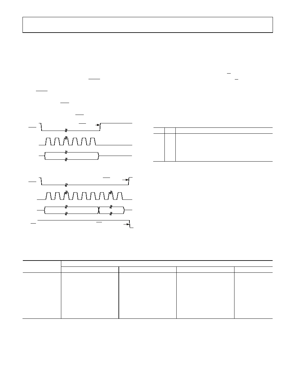
PACKET ERROR CHECKING
To verify that data has been received correctly in noisy environ-
ments, the AD5362/AD5363 offer the option of error checking
based on an 8-bit (CRC-8) cyclic redundancy check. The device
controlling the AD5362/AD5363 should generate an 8-bit
checksum using the polynomial C(x) = x8 + x2 + x1 + 1. This is
added to the end of the data-word, and 32 data bits are sent to
the AD5362/AD5363 before taking SYNC high. If the AD5362/
AD5363 see a 32-bit data frame, an error check is performed
when SYNC goes high. If the checksum is valid, the data is
written to the selected register. If the checksum is invalid, the
packet error check (PEC) output goes low and Bit 3 of the
control register is set. After reading the control register, Bit 3
is cleared automatically and PEC goes high again.
SYNC
SCLK
SDI
24-BIT DATA TRANSFER—NO ERROR CHECKING
SYNC
SCLK
SDI
MSB
D23
LSB
D0
MSB
D31
LSB
D8
D7
D0
UPDATE ON SYNC HIGH
UPDATE AFTER SYNC HIGH
ONLY IF ERROR CHECK PASSED
24-BIT DATA
24-BIT DATA TRANSFER WITH ERROR CHECKING
8-BIT FCS
PEC
PEC GOES LOW IF
ERROR CHECK FAILS
05
76
2-
02
6
Figure 24. SPI Write With and Without Error Checking
CHANNEL ADDRESSING AND SPECIAL MODES
If the mode bits are not 00, the data-word D15 to D0 (AD5362)
or D13 to D0 (AD5363) is written to the device. Address Bit A4
to Address Bit A0 determine which channels are written to, and
the mode bits determine to which register (X1A, X1B, C, or M)
be written to the X1A register when the A/B bit in the control
register is 0, or to the X1B register when the A/B bit is 1.
The AD5362/AD5363 have very flexible addressing that allows
the writing of data to a single channel, all channels in a group,
or all channels in the device.
Table 14 shows which groups and which channels are addressed
for every combination of Address Bit A4 to Address Bit A0.
Table 13. Mode Bits
M1
M0
Action
1
Write to DAC data (X) register
1
0
Write to DAC offset (C) register
0
1
Write to DAC gain (M) register
0
Special function, used in combination with other
bits of the data-word
Table 14. Group and Channel Addressing
Address Bit A2
to Address Bit A0
Address Bit A4 to Address Bit A3
00
01
10
11
000
All groups, all channels
Group 0, Channel 0
Group 1, Channel 0
Unused
001
Group 0, all channels
Group 0, Channel 1
Group 1, Channel 1
Unused
010
Group 1, all channels
Group 0, Channel 2
Group 1, Channel 2
Unused
011
Unused
Group 0, Channel 3
Group 1, Channel 3
Unused
100
Unused
101
Unused
110
Unused
111
Unused
相关PDF资料 |
PDF描述 |
|---|---|
| LTC1596AISW#TRPBF | IC D/A CONV 16BIT MLTPLYNG16SOIC |
| LTC1596AISW#TR | IC DAC 16BIT MULTIPLY SER 16SOIC |
| LTC1596-1AISW#TRPBF | IC D/A CONV 16BIT MLTPLYNG16SOIC |
| LTC1596-1AISW#TR | IC DAC 16BIT MULTIPLY SER 16SOIC |
| AD7237AAN | IC DAC 12BIT W/AMP W/BUFF 24-DIP |
相关代理商/技术参数 |
参数描述 |
|---|---|
| AD5363BCPZ-REEL7 | 功能描述:IC DAC 14BIT 8CH SERIAL 56-LFCSP RoHS:是 类别:集成电路 (IC) >> 数据采集 - 数模转换器 系列:- 产品培训模块:Data Converter Fundamentals DAC Architectures 标准包装:750 系列:- 设置时间:7µs 位数:16 数据接口:并联 转换器数目:1 电压电源:双 ± 功率耗散(最大):100mW 工作温度:0°C ~ 70°C 安装类型:表面贴装 封装/外壳:28-LCC(J 形引线) 供应商设备封装:28-PLCC(11.51x11.51) 包装:带卷 (TR) 输出数目和类型:1 电压,单极;1 电压,双极 采样率(每秒):143k |
| AD5363BSTZ | 功能描述:IC DAC 14BIT 8CH SERIAL 52-LQFP RoHS:是 类别:集成电路 (IC) >> 数据采集 - 数模转换器 系列:- 产品培训模块:Data Converter Fundamentals DAC Architectures 标准包装:750 系列:- 设置时间:7µs 位数:16 数据接口:并联 转换器数目:1 电压电源:双 ± 功率耗散(最大):100mW 工作温度:0°C ~ 70°C 安装类型:表面贴装 封装/外壳:28-LCC(J 形引线) 供应商设备封装:28-PLCC(11.51x11.51) 包装:带卷 (TR) 输出数目和类型:1 电压,单极;1 电压,双极 采样率(每秒):143k |
| AD5363BSTZ-REEL | 功能描述:IC DAC 14BIT 8CH SERIAL 52-LQFP RoHS:是 类别:集成电路 (IC) >> 数据采集 - 数模转换器 系列:- 产品培训模块:Data Converter Fundamentals DAC Architectures 标准包装:750 系列:- 设置时间:7µs 位数:16 数据接口:并联 转换器数目:1 电压电源:双 ± 功率耗散(最大):100mW 工作温度:0°C ~ 70°C 安装类型:表面贴装 封装/外壳:28-LCC(J 形引线) 供应商设备封装:28-PLCC(11.51x11.51) 包装:带卷 (TR) 输出数目和类型:1 电压,单极;1 电压,双极 采样率(每秒):143k |
| AD5365D/BIN/883B | 制造商:Analog Devices 功能描述:- Rail/Tube |
| AD536A | 制造商:AD 制造商全称:Analog Devices 功能描述:Integrated Circuit True RMS-to-DC Converter |
发布紧急采购,3分钟左右您将得到回复。