参数资料
| 型号: | AD5392BSTZ-5 |
| 厂商: | Analog Devices Inc |
| 文件页数: | 16/44页 |
| 文件大小: | 0K |
| 描述: | IC DAC 14BIT 8CHAN 3V 52LQFP |
| 产品培训模块: | Data Converter Fundamentals DAC Architectures |
| 产品变化通告: | AD5390/1/2 Redesign Change 16/May/2012 |
| 设计资源: | 8 to 16 Channels of Programmable Voltage with Excellent Temperature Drift Performance Using AD5390/1/2 (CN0029) AD5390/91/92 Channel Monitor Function (CN0030) |
| 标准包装: | 1 |
| 设置时间: | 8µs |
| 位数: | 14 |
| 数据接口: | I²C,串行 |
| 转换器数目: | 16 |
| 电压电源: | 单电源 |
| 功率耗散(最大): | 35mW |
| 工作温度: | -40°C ~ 85°C |
| 安装类型: | 表面贴装 |
| 封装/外壳: | 52-LQFP |
| 供应商设备封装: | 52-LQFP(10x10) |
| 包装: | 托盘 |
| 输出数目和类型: | 8 电压,单极 |
| 采样率(每秒): | 125k |
第1页第2页第3页第4页第5页第6页第7页第8页第9页第10页第11页第12页第13页第14页第15页当前第16页第17页第18页第19页第20页第21页第22页第23页第24页第25页第26页第27页第28页第29页第30页第31页第32页第33页第34页第35页第36页第37页第38页第39页第40页第41页第42页第43页第44页
Data Sheet
AD5390/AD5391/AD5392
Rev. E | Page 23 of 44
FUNCTIONAL DESCRIPTION
DAC ARCHITECTURE
The AD5390/AD5391 are complete single-supply, 16-channel,
voltage output DACs offering a resolution of 14 bits and 12 bits,
respectively. The AD5392 is a complete single-supply, 8-channel,
voltage output DAC offering 14-bit resolution. All devices are
available in a 64-lead LFCSP and 52-lead LQFP, and feature
serial interfaces. This family includes an internal select-able
1.25 V/2.5 V, 10 ppm/°C reference that can be used to drive the
buffered reference inputs (alternatively, an external reference
can be used to drive these inputs). All channels have an on-chip
output amplifier with rail-to-rail output capable of driving a
5 kΩ load in parallel with a 200 pF capacitance.
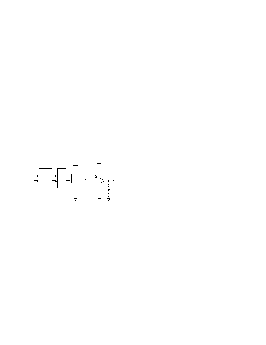
The architecture of a single DAC channel consists of a 12-bit
and 14-bit resistor-string DAC followed by an output buffer
amplifier operating at a gain of 2. This resistor-string architecture
guarantees DAC monotonicity. The 12-bit and 14-bit binary
digital code loaded to the DAC register determines at what
node on the string the voltage is tapped off before being fed to
the output amplifier. Each channel on these devices contains
independent offset and gain control registers, allowing the user
to digitally trim offset and gain.
x1 INPUT
REG
m REG
c REG
x2
DAC
REG
14-BIT
DAC
INPUT
DATA
R
AVDD
VOUT
VREF
03773-
018
Figure 31. Single-Channel Architecture
These registers let the user calibrate out errors in the complete
signal chain including the DAC using the internal m and c
registers, which hold the correction factors. All channels are
double-buffered, allowing synchronous updating of all channels
using the LDAC pin. Figure 31 shows a block diagram of a
single channel on the AD5390/AD5391/AD5392.
The digital input transfer function for each DAC can be
represented as
(
)
(
)
(
)1
2
1
2
/
2
+
×
+
=
n
c
x
m
x
where:
x2 is the data-word loaded to the resistor-string DAC.
x1 is the 12-bit and 14-bit data-word written to the DAC input
register.
m is the 12-bit and 14-bit gain coefficient (default is all 0x3FFE
on the AD5390/AD5392 and 0xFFE on the AD5391). The LSB
of the gain coefficient is zero.
n = DAC resolution (n = 14 for the AD5390/AD5392 and
n = 12 for the AD5391).
c is the 12-bit and 14-bit offset coefficient (default is 0x2000 on
the AD5390/AD5392 and 0x800 on the AD5391).
The complete transfer function for these devices can be
represented as
n
x
VREF
VOUT
2
/
2
×
=
where:
x2 is the data-word loaded to the resistor-string DAC.
VREF is the reference voltage applied to the REFIN/REFOUT pin
on the DAC when an external reference is used (2.5 V for specified
performance on the AD539x-5 products and 1.25 V on the
AD539x-3 products).
相关PDF资料 |
PDF描述 |
|---|---|
| MS27473T20B35PLC | CONN HSG PLUG 79POS STRGHT PIN |
| VE-2WP-MY-F1 | CONVERTER MOD DC/DC 13.8V 50W |
| AD669ARZ | IC DAC 16BIT MONO W/VREF 28-SOIC |
| VI-BW0-MV-F2 | CONVERTER MOD DC/DC 5V 150W |
| MS27496E23F53S | CONN RCPT 53POS BOX MNT W/SCKT |
相关代理商/技术参数 |
参数描述 |
|---|---|
| AD5398ABCBZ-REEL | 功能描述:IC DAC 10BIT CURRENT-SINK 9WLCSP RoHS:是 类别:集成电路 (IC) >> 数据采集 - 数模转换器 系列:- 产品培训模块:Data Converter Fundamentals DAC Architectures 设计资源:Unipolar, Precision DC Digital-to-Analog Conversion using AD5450/1/2/3 8-14-Bit DACs (CN0052) Precision, Bipolar, Configuration for AD5450/1/2/3 8-14bit Multiplying DACs (CN0053) AC Signal Processing Using AD5450/1/2/3 Current Output DACs (CN0054) Programmable Gain Element Using AD5450/1/2/3 Current Output DAC Family (CN0055) Single Supply Low Noise LED Current Source Driver Using a Current Output DAC in the Reverse Mode (CN0139) 标准包装:10,000 系列:- 设置时间:- 位数:12 数据接口:DSP,MICROWIRE?,QSPI?,串行,SPI? 转换器数目:1 电压电源:单电源 功率耗散(最大):- 工作温度:-40°C ~ 125°C 安装类型:表面贴装 封装/外壳:SOT-23-8 薄型,TSOT-23-8 供应商设备封装:TSOT-23-8 包装:带卷 (TR) 输出数目和类型:1 电流,单极;1 电流,双极 采样率(每秒):2.7M |
| AD5398ABCBZ-REEL7 | 功能描述:IC DAC 10BIT CURRENT-SINK 9WLCSP RoHS:是 类别:集成电路 (IC) >> 数据采集 - 数模转换器 系列:- 产品培训模块:Lead (SnPb) Finish for COTS Obsolescence Mitigation Program 标准包装:50 系列:- 设置时间:4µs 位数:12 数据接口:串行 转换器数目:2 电压电源:单电源 功率耗散(最大):- 工作温度:-40°C ~ 85°C 安装类型:表面贴装 封装/外壳:8-TSSOP,8-MSOP(0.118",3.00mm 宽) 供应商设备封装:8-uMAX 包装:管件 输出数目和类型:2 电压,单极 采样率(每秒):* 产品目录页面:1398 (CN2011-ZH PDF) |
| AD5398A-WAFER | 功能描述:10 Bit Digital to Analog Converter 1 9-WLCSP (1.52 x 1.69) 制造商:analog devices inc. 系列:- 包装:散装 零件状态:上次购买时间 位数:10 数模转换器数:1 建立时间:250μs(标准) 输出类型:Current - Unbuffered 差分输出:无 数据接口:I2C 参考类型:内部 电压 - 电源,模拟:2.7 V ~ 5.5 V 电压 - 电源,数字:2.7 V ~ 5.5 V INL/DNL(LSB):±1.5,±1(最大) 架构:电流阱 工作温度:-30°C ~ 85°C 封装/外壳:9-UFBGA,WLCSP 供应商器件封装:9-WLCSP(1.52 x 1.69) 标准包装:1 |
| AD5398BCBZ-REEL | 功能描述:IC DAC 10BIT CURRENT-SINK 9WLCSP RoHS:是 类别:集成电路 (IC) >> 数据采集 - 数模转换器 系列:- 标准包装:2,400 系列:- 设置时间:- 位数:18 数据接口:串行 转换器数目:3 电压电源:模拟和数字 功率耗散(最大):- 工作温度:-40°C ~ 85°C 安装类型:表面贴装 封装/外壳:36-TFBGA 供应商设备封装:36-TFBGA 包装:带卷 (TR) 输出数目和类型:* 采样率(每秒):* |
| AD5398BCBZ-REEL7 | 功能描述:IC DAC 10BIT CURRENT-SINK 9WLCSP RoHS:是 类别:集成电路 (IC) >> 数据采集 - 数模转换器 系列:- 产品培训模块:Lead (SnPb) Finish for COTS Obsolescence Mitigation Program 标准包装:50 系列:- 设置时间:4µs 位数:12 数据接口:串行 转换器数目:2 电压电源:单电源 功率耗散(最大):- 工作温度:-40°C ~ 85°C 安装类型:表面贴装 封装/外壳:8-TSSOP,8-MSOP(0.118",3.00mm 宽) 供应商设备封装:8-uMAX 包装:管件 输出数目和类型:2 电压,单极 采样率(每秒):* 产品目录页面:1398 (CN2011-ZH PDF) |
发布紧急采购,3分钟左右您将得到回复。