参数资料
| 型号: | AD5392BSTZ-5 |
| 厂商: | Analog Devices Inc |
| 文件页数: | 33/44页 |
| 文件大小: | 0K |
| 描述: | IC DAC 14BIT 8CHAN 3V 52LQFP |
| 产品培训模块: | Data Converter Fundamentals DAC Architectures |
| 产品变化通告: | AD5390/1/2 Redesign Change 16/May/2012 |
| 设计资源: | 8 to 16 Channels of Programmable Voltage with Excellent Temperature Drift Performance Using AD5390/1/2 (CN0029) AD5390/91/92 Channel Monitor Function (CN0030) |
| 标准包装: | 1 |
| 设置时间: | 8µs |
| 位数: | 14 |
| 数据接口: | I²C,串行 |
| 转换器数目: | 16 |
| 电压电源: | 单电源 |
| 功率耗散(最大): | 35mW |
| 工作温度: | -40°C ~ 85°C |
| 安装类型: | 表面贴装 |
| 封装/外壳: | 52-LQFP |
| 供应商设备封装: | 52-LQFP(10x10) |
| 包装: | 托盘 |
| 输出数目和类型: | 8 电压,单极 |
| 采样率(每秒): | 125k |
第1页第2页第3页第4页第5页第6页第7页第8页第9页第10页第11页第12页第13页第14页第15页第16页第17页第18页第19页第20页第21页第22页第23页第24页第25页第26页第27页第28页第29页第30页第31页第32页当前第33页第34页第35页第36页第37页第38页第39页第40页第41页第42页第43页第44页
Data Sheet
AD5390/AD5391/AD5392
Rev. E | Page 39 of 44
Power Amplifier Control
Multistage power amplifier designs require a large number of
setpoints in the operation and control of the output stage. The
AD539x are ideal for these applications because of their small
size (LFCSP) and the integration of 8 and 16 channels, offering
12- and 14-bit resolution. Figure 45 shows a typical transmitter
architecture, in which the AD539x DACs can be used in the
following control circuits: IBIAS control, average power control
(APC), peak power control (PPC), transmit gain control (TGC),
and audio level control (ALC). DACs are also required for
variable voltage attenuators, phase shifter control, and dc-
setpoint control in the overall amplifier design.
03773-
032
POWER
AMPLIFIER
EXCITER
AUDIO
SOURCE
50
LOAD
PHASE
SHIFT
IBIAS
TGC
APC
PPC
ALC
Figure 45. Multistage Power Amplifier Control
Process Control Applications
The AD539x-5 family is ideal for process control applications
because it offers a combination of 8 and 16 channels and 12-bit
and 14-bit resolution. These applications generally require
output voltage ranges of 0 V to 5 V ± 5 V, 0 V to 10 V ± 10 V,
and current sink and source functions. The AD539x-5 products
operate from a single 5 V supply and, therefore, require external
signal conditioning to achieve the output ranges described here.
Figure 46 shows configurations to achieve these output ranges.
The key advantages of using AD539x-5 products in these
applications are small package size, pin compatibility with the
ability to upgrade from 12 to 14 bits, integrated on-chip 2.5 V
reference with 10 ppm/°C maximum temperature coefficient,
and excellent accuracy specifications. The AD539x-5 family
contains an offset and gain register for each channel, so users
can perform system-level calibration on a per-channel basis.
03773-
033
VOUT 3
2.5V
REFERENCE
±10V
RANGE
±5V
RANGE
4R
AD539x-5
VOUT 0
VOUT 1
VOUT 2
VOUT 4
0.1F
R
4R
2R
I SINK
R1
R
1/4 OP747/
1/4 OP4177
1/4 OP747/
1/4 OP4177
1/4 OP747/
1/4 OP4177
1/4 OP747/
1/4 OP4177
0V TO 10V
RANGE
0V TO 5V
RANGE
Figure 46. Output Configurations for Process Control Applications
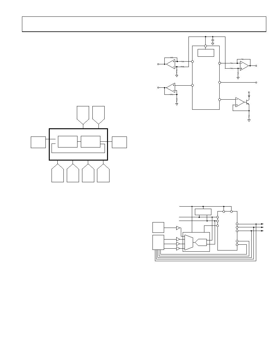
Optical Transceivers
The AD539x-3 family of products are ideally suited to optical
transceiver applications. In 300-pin MSA applications, for
example, digital-to-analog converters are required to control the
laser power, APD bias, and modulator amplitude. Diagnostic
information is required as analog outputs from the module. The
AD539x-3 products offer a combination of 8/16 channels, a
resolution of 12/14 bits in a 64-lead LFCSP, and operate from a
supply voltage of 2.7 V to 5.5 V supply with internal reference.
The AD539x-3 parts also feature I2C-compatible and SPI inter-
faces, making them ideal components for use in these applications.
Figure 47 shows a typical configuration in an optical transceiver
application.
10G LDD
AND
LASER
PIN/APD
AND TIA
IRXP
IMODMON
IMPD
IBIASMON
AIN
MUX
SDA
VLSRBIAS
VLSRPWRMON
VXLOPMON
IBIAS
IMOD
SCL
REFOUT/REFIN
AD539x-3
AVDD
DVDD
AVDD
REFIN
AD7994
12-BIT
ADC
TIAs
I2C
BUS
3V
CONTROLLER
SDA
SCL
03773-
062
Figure 47. Optical Transceiver using the AD539x-3
相关PDF资料 |
PDF描述 |
|---|---|
| MS27473T20B35PLC | CONN HSG PLUG 79POS STRGHT PIN |
| VE-2WP-MY-F1 | CONVERTER MOD DC/DC 13.8V 50W |
| AD669ARZ | IC DAC 16BIT MONO W/VREF 28-SOIC |
| VI-BW0-MV-F2 | CONVERTER MOD DC/DC 5V 150W |
| MS27496E23F53S | CONN RCPT 53POS BOX MNT W/SCKT |
相关代理商/技术参数 |
参数描述 |
|---|---|
| AD5398ABCBZ-REEL | 功能描述:IC DAC 10BIT CURRENT-SINK 9WLCSP RoHS:是 类别:集成电路 (IC) >> 数据采集 - 数模转换器 系列:- 产品培训模块:Data Converter Fundamentals DAC Architectures 设计资源:Unipolar, Precision DC Digital-to-Analog Conversion using AD5450/1/2/3 8-14-Bit DACs (CN0052) Precision, Bipolar, Configuration for AD5450/1/2/3 8-14bit Multiplying DACs (CN0053) AC Signal Processing Using AD5450/1/2/3 Current Output DACs (CN0054) Programmable Gain Element Using AD5450/1/2/3 Current Output DAC Family (CN0055) Single Supply Low Noise LED Current Source Driver Using a Current Output DAC in the Reverse Mode (CN0139) 标准包装:10,000 系列:- 设置时间:- 位数:12 数据接口:DSP,MICROWIRE?,QSPI?,串行,SPI? 转换器数目:1 电压电源:单电源 功率耗散(最大):- 工作温度:-40°C ~ 125°C 安装类型:表面贴装 封装/外壳:SOT-23-8 薄型,TSOT-23-8 供应商设备封装:TSOT-23-8 包装:带卷 (TR) 输出数目和类型:1 电流,单极;1 电流,双极 采样率(每秒):2.7M |
| AD5398ABCBZ-REEL7 | 功能描述:IC DAC 10BIT CURRENT-SINK 9WLCSP RoHS:是 类别:集成电路 (IC) >> 数据采集 - 数模转换器 系列:- 产品培训模块:Lead (SnPb) Finish for COTS Obsolescence Mitigation Program 标准包装:50 系列:- 设置时间:4µs 位数:12 数据接口:串行 转换器数目:2 电压电源:单电源 功率耗散(最大):- 工作温度:-40°C ~ 85°C 安装类型:表面贴装 封装/外壳:8-TSSOP,8-MSOP(0.118",3.00mm 宽) 供应商设备封装:8-uMAX 包装:管件 输出数目和类型:2 电压,单极 采样率(每秒):* 产品目录页面:1398 (CN2011-ZH PDF) |
| AD5398A-WAFER | 功能描述:10 Bit Digital to Analog Converter 1 9-WLCSP (1.52 x 1.69) 制造商:analog devices inc. 系列:- 包装:散装 零件状态:上次购买时间 位数:10 数模转换器数:1 建立时间:250μs(标准) 输出类型:Current - Unbuffered 差分输出:无 数据接口:I2C 参考类型:内部 电压 - 电源,模拟:2.7 V ~ 5.5 V 电压 - 电源,数字:2.7 V ~ 5.5 V INL/DNL(LSB):±1.5,±1(最大) 架构:电流阱 工作温度:-30°C ~ 85°C 封装/外壳:9-UFBGA,WLCSP 供应商器件封装:9-WLCSP(1.52 x 1.69) 标准包装:1 |
| AD5398BCBZ-REEL | 功能描述:IC DAC 10BIT CURRENT-SINK 9WLCSP RoHS:是 类别:集成电路 (IC) >> 数据采集 - 数模转换器 系列:- 标准包装:2,400 系列:- 设置时间:- 位数:18 数据接口:串行 转换器数目:3 电压电源:模拟和数字 功率耗散(最大):- 工作温度:-40°C ~ 85°C 安装类型:表面贴装 封装/外壳:36-TFBGA 供应商设备封装:36-TFBGA 包装:带卷 (TR) 输出数目和类型:* 采样率(每秒):* |
| AD5398BCBZ-REEL7 | 功能描述:IC DAC 10BIT CURRENT-SINK 9WLCSP RoHS:是 类别:集成电路 (IC) >> 数据采集 - 数模转换器 系列:- 产品培训模块:Lead (SnPb) Finish for COTS Obsolescence Mitigation Program 标准包装:50 系列:- 设置时间:4µs 位数:12 数据接口:串行 转换器数目:2 电压电源:单电源 功率耗散(最大):- 工作温度:-40°C ~ 85°C 安装类型:表面贴装 封装/外壳:8-TSSOP,8-MSOP(0.118",3.00mm 宽) 供应商设备封装:8-uMAX 包装:管件 输出数目和类型:2 电压,单极 采样率(每秒):* 产品目录页面:1398 (CN2011-ZH PDF) |
发布紧急采购,3分钟左右您将得到回复。