参数资料
| 型号: | AD5392BSTZ-5 |
| 厂商: | Analog Devices Inc |
| 文件页数: | 31/44页 |
| 文件大小: | 0K |
| 描述: | IC DAC 14BIT 8CHAN 3V 52LQFP |
| 产品培训模块: | Data Converter Fundamentals DAC Architectures |
| 产品变化通告: | AD5390/1/2 Redesign Change 16/May/2012 |
| 设计资源: | 8 to 16 Channels of Programmable Voltage with Excellent Temperature Drift Performance Using AD5390/1/2 (CN0029) AD5390/91/92 Channel Monitor Function (CN0030) |
| 标准包装: | 1 |
| 设置时间: | 8µs |
| 位数: | 14 |
| 数据接口: | I²C,串行 |
| 转换器数目: | 16 |
| 电压电源: | 单电源 |
| 功率耗散(最大): | 35mW |
| 工作温度: | -40°C ~ 85°C |
| 安装类型: | 表面贴装 |
| 封装/外壳: | 52-LQFP |
| 供应商设备封装: | 52-LQFP(10x10) |
| 包装: | 托盘 |
| 输出数目和类型: | 8 电压,单极 |
| 采样率(每秒): | 125k |
第1页第2页第3页第4页第5页第6页第7页第8页第9页第10页第11页第12页第13页第14页第15页第16页第17页第18页第19页第20页第21页第22页第23页第24页第25页第26页第27页第28页第29页第30页当前第31页第32页第33页第34页第35页第36页第37页第38页第39页第40页第41页第42页第43页第44页
Data Sheet
AD5390/AD5391/AD5392
Rev. E | Page 37 of 44
APPLICATION INFORMATION
POWER SUPPLY DECOUPLING
In any circuit where accuracy is important, careful
consideration of the power supply and ground return layout
helps to ensure the rated performance. The printed circuit
board on which the AD539x is mounted should be designed so
that the analog and digital sections are separated and confined
to certain areas of the board. If the AD539x is in a system where
multiple devices require an AGND-to-DGND connection, the
connection should be made at one point only. The star ground
point should be established as close as possible to the device.
For supplies with multiple pins (AVDD, AVCC), it is recom-
mended to tie those pins together. The AD539x should have
ample supply bypassing of 10 F in parallel with 0.1 F on each
supply located as close to the package as possible—ideally right
up against the device. The 10 F capacitors are the tantalum
bead type. The 0.1 F capacitor should have low effective series
resistance (ESR) and effective series inductance (ESI), such as
the common ceramic types that provide a low impedance path
to ground at high frequencies, to handle transient currents due
to internal logic switching.
The power supply lines of the AD539x should use as large a
trace as possible to provide low impedance paths and reduce
the effects of glitches on the power supply line. Fast switching
signals such as clocks should be shielded with digital ground
to avoid radiating noise to other parts of the board, and should
never run near the reference inputs. A ground line routed
between the DIN and SCLK lines helps reduce crosstalk
between them (not required on a multilayer board, because
there is a separate ground plane, but separating the lines helps).
Avoid crossover of digital and analog signals. Traces on
opposite sides of the board should run at right angles to each
other. This reduces the effects of feedthrough through the
board. A micro-strip technique is by far the best, but not always
possible with a double-sided board. In this technique, the
component side of the board is dedicated to ground plane,
while signal traces are placed on the soldered side.
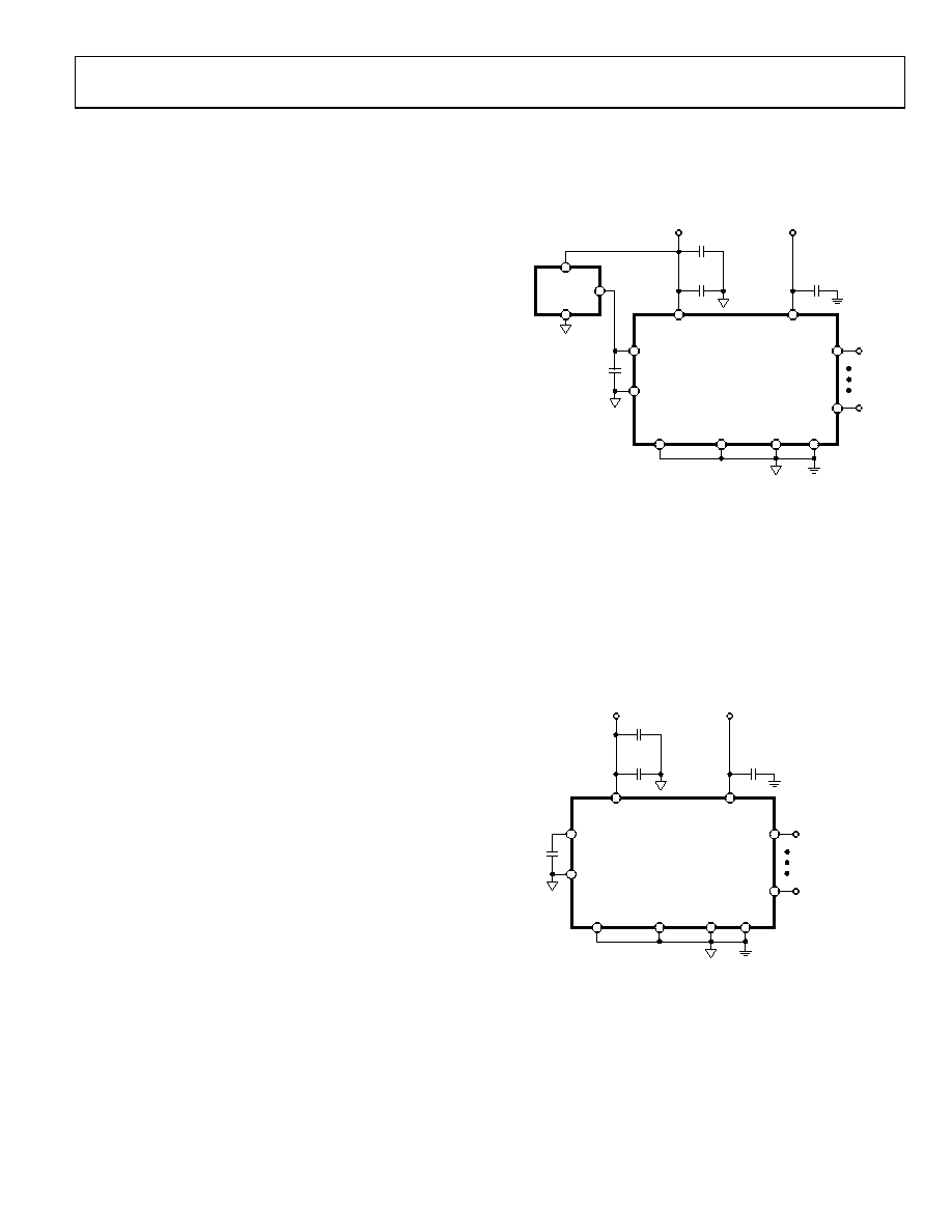
TYPICAL CONFIGURATION CIRCUIT
Figure 41 shows a typical configuration for the AD539x when
configured for use with an external reference. In the circuit
shown, all AGND, SIGNAL_GND, and DAC_GND pins are
tied together to a common AGND. AGND and DGND are
connected together at the AD539x device. On power-up,
the AD539x defaults to external reference operation. All
AVDD lines are connected together and driven from the same
5 V source. It is recommended to decouple close to the device
with a 0.1 F ceramic and a 10 F tantalum capacitor. In this
application, the reference for the AD539x-5 is provided
externally from either an ADR421 or ADR431 2.5 V reference.
Suitable external references for the AD539x-3 include the
ADR280 1.2 V reference. The reference should be decoupled at
the REFOUT/REFIN pin of the device with a 0.1 F capacitor.
03773-
061
ADR431/
ADR421
AD539x
AVDD
DVDD
SIGNAL_GND
DAC_GND
DGND
VOUT 15
VOUT 0
AGND
REFOUT/REFIN
REF_GND
0.1F
10F
0.1F
AVDD
DVDD
Figure 41. Typical Configuration with External Reference
Figure 42 shows a typical configuration when using the internal
reference. On power-up, the AD539x defaults to an external
reference; therefore, the internal reference needs to be configured
and turned on via a write to the AD539x control register. On the
AD5390/AD5392, Control Register Bit CR12 lets the user choose
the reference voltage; Bit CR10 is used to select the internal
reference. It is recommended to use the 2.5 V reference when
AVDD = 5 V, and the 1.25 V reference when AVDD = 3 V. On the
AD5391, Control Register Bit CR10 lets the user choose the ref-
erence voltage; Bit CR8 is used to select the internal reference.
03773-
060
AD539x
AVDD
DVDD
SIGNAL_GND
DAC_GND
DGND
VOUT 15
VOUT 0
AGND
REFOUT/REFIN
REF_GND
0.1F
10F
0.1F
AVDD
DVDD
Figure 42. Typical Configuration with Internal Reference.
(Digital Connections Omitted for Clarity)
The AD539x contains an internal power-on reset circuit with a
10 ms brown-out time. If the power supply ramp rate exceeds
10 ms, the user should reset the AD539x as part of the initiali-
zation process to ensure the calibration data is loaded correctly
into the device.
相关PDF资料 |
PDF描述 |
|---|---|
| MS27473T20B35PLC | CONN HSG PLUG 79POS STRGHT PIN |
| VE-2WP-MY-F1 | CONVERTER MOD DC/DC 13.8V 50W |
| AD669ARZ | IC DAC 16BIT MONO W/VREF 28-SOIC |
| VI-BW0-MV-F2 | CONVERTER MOD DC/DC 5V 150W |
| MS27496E23F53S | CONN RCPT 53POS BOX MNT W/SCKT |
相关代理商/技术参数 |
参数描述 |
|---|---|
| AD5398ABCBZ-REEL | 功能描述:IC DAC 10BIT CURRENT-SINK 9WLCSP RoHS:是 类别:集成电路 (IC) >> 数据采集 - 数模转换器 系列:- 产品培训模块:Data Converter Fundamentals DAC Architectures 设计资源:Unipolar, Precision DC Digital-to-Analog Conversion using AD5450/1/2/3 8-14-Bit DACs (CN0052) Precision, Bipolar, Configuration for AD5450/1/2/3 8-14bit Multiplying DACs (CN0053) AC Signal Processing Using AD5450/1/2/3 Current Output DACs (CN0054) Programmable Gain Element Using AD5450/1/2/3 Current Output DAC Family (CN0055) Single Supply Low Noise LED Current Source Driver Using a Current Output DAC in the Reverse Mode (CN0139) 标准包装:10,000 系列:- 设置时间:- 位数:12 数据接口:DSP,MICROWIRE?,QSPI?,串行,SPI? 转换器数目:1 电压电源:单电源 功率耗散(最大):- 工作温度:-40°C ~ 125°C 安装类型:表面贴装 封装/外壳:SOT-23-8 薄型,TSOT-23-8 供应商设备封装:TSOT-23-8 包装:带卷 (TR) 输出数目和类型:1 电流,单极;1 电流,双极 采样率(每秒):2.7M |
| AD5398ABCBZ-REEL7 | 功能描述:IC DAC 10BIT CURRENT-SINK 9WLCSP RoHS:是 类别:集成电路 (IC) >> 数据采集 - 数模转换器 系列:- 产品培训模块:Lead (SnPb) Finish for COTS Obsolescence Mitigation Program 标准包装:50 系列:- 设置时间:4µs 位数:12 数据接口:串行 转换器数目:2 电压电源:单电源 功率耗散(最大):- 工作温度:-40°C ~ 85°C 安装类型:表面贴装 封装/外壳:8-TSSOP,8-MSOP(0.118",3.00mm 宽) 供应商设备封装:8-uMAX 包装:管件 输出数目和类型:2 电压,单极 采样率(每秒):* 产品目录页面:1398 (CN2011-ZH PDF) |
| AD5398A-WAFER | 功能描述:10 Bit Digital to Analog Converter 1 9-WLCSP (1.52 x 1.69) 制造商:analog devices inc. 系列:- 包装:散装 零件状态:上次购买时间 位数:10 数模转换器数:1 建立时间:250μs(标准) 输出类型:Current - Unbuffered 差分输出:无 数据接口:I2C 参考类型:内部 电压 - 电源,模拟:2.7 V ~ 5.5 V 电压 - 电源,数字:2.7 V ~ 5.5 V INL/DNL(LSB):±1.5,±1(最大) 架构:电流阱 工作温度:-30°C ~ 85°C 封装/外壳:9-UFBGA,WLCSP 供应商器件封装:9-WLCSP(1.52 x 1.69) 标准包装:1 |
| AD5398BCBZ-REEL | 功能描述:IC DAC 10BIT CURRENT-SINK 9WLCSP RoHS:是 类别:集成电路 (IC) >> 数据采集 - 数模转换器 系列:- 标准包装:2,400 系列:- 设置时间:- 位数:18 数据接口:串行 转换器数目:3 电压电源:模拟和数字 功率耗散(最大):- 工作温度:-40°C ~ 85°C 安装类型:表面贴装 封装/外壳:36-TFBGA 供应商设备封装:36-TFBGA 包装:带卷 (TR) 输出数目和类型:* 采样率(每秒):* |
| AD5398BCBZ-REEL7 | 功能描述:IC DAC 10BIT CURRENT-SINK 9WLCSP RoHS:是 类别:集成电路 (IC) >> 数据采集 - 数模转换器 系列:- 产品培训模块:Lead (SnPb) Finish for COTS Obsolescence Mitigation Program 标准包装:50 系列:- 设置时间:4µs 位数:12 数据接口:串行 转换器数目:2 电压电源:单电源 功率耗散(最大):- 工作温度:-40°C ~ 85°C 安装类型:表面贴装 封装/外壳:8-TSSOP,8-MSOP(0.118",3.00mm 宽) 供应商设备封装:8-uMAX 包装:管件 输出数目和类型:2 电压,单极 采样率(每秒):* 产品目录页面:1398 (CN2011-ZH PDF) |
发布紧急采购,3分钟左右您将得到回复。