参数资料
| 型号: | AD5392BSTZ-5 |
| 厂商: | Analog Devices Inc |
| 文件页数: | 25/44页 |
| 文件大小: | 0K |
| 描述: | IC DAC 14BIT 8CHAN 3V 52LQFP |
| 产品培训模块: | Data Converter Fundamentals DAC Architectures |
| 产品变化通告: | AD5390/1/2 Redesign Change 16/May/2012 |
| 设计资源: | 8 to 16 Channels of Programmable Voltage with Excellent Temperature Drift Performance Using AD5390/1/2 (CN0029) AD5390/91/92 Channel Monitor Function (CN0030) |
| 标准包装: | 1 |
| 设置时间: | 8µs |
| 位数: | 14 |
| 数据接口: | I²C,串行 |
| 转换器数目: | 16 |
| 电压电源: | 单电源 |
| 功率耗散(最大): | 35mW |
| 工作温度: | -40°C ~ 85°C |
| 安装类型: | 表面贴装 |
| 封装/外壳: | 52-LQFP |
| 供应商设备封装: | 52-LQFP(10x10) |
| 包装: | 托盘 |
| 输出数目和类型: | 8 电压,单极 |
| 采样率(每秒): | 125k |
第1页第2页第3页第4页第5页第6页第7页第8页第9页第10页第11页第12页第13页第14页第15页第16页第17页第18页第19页第20页第21页第22页第23页第24页当前第25页第26页第27页第28页第29页第30页第31页第32页第33页第34页第35页第36页第37页第38页第39页第40页第41页第42页第43页第44页
Data Sheet
AD5390/AD5391/AD5392
Rev. E | Page 31 of 44
AD539x ON-CHIP SPECIAL FUNCTION REGISTERS
The AD539x family of parts contains a number of special
function registers (SFRs) as shown in Table 22. SFRs are
addressed with REG1 = 0 and REG0 = 0 and are decoded
using Address Bit A3 to Bit A0.
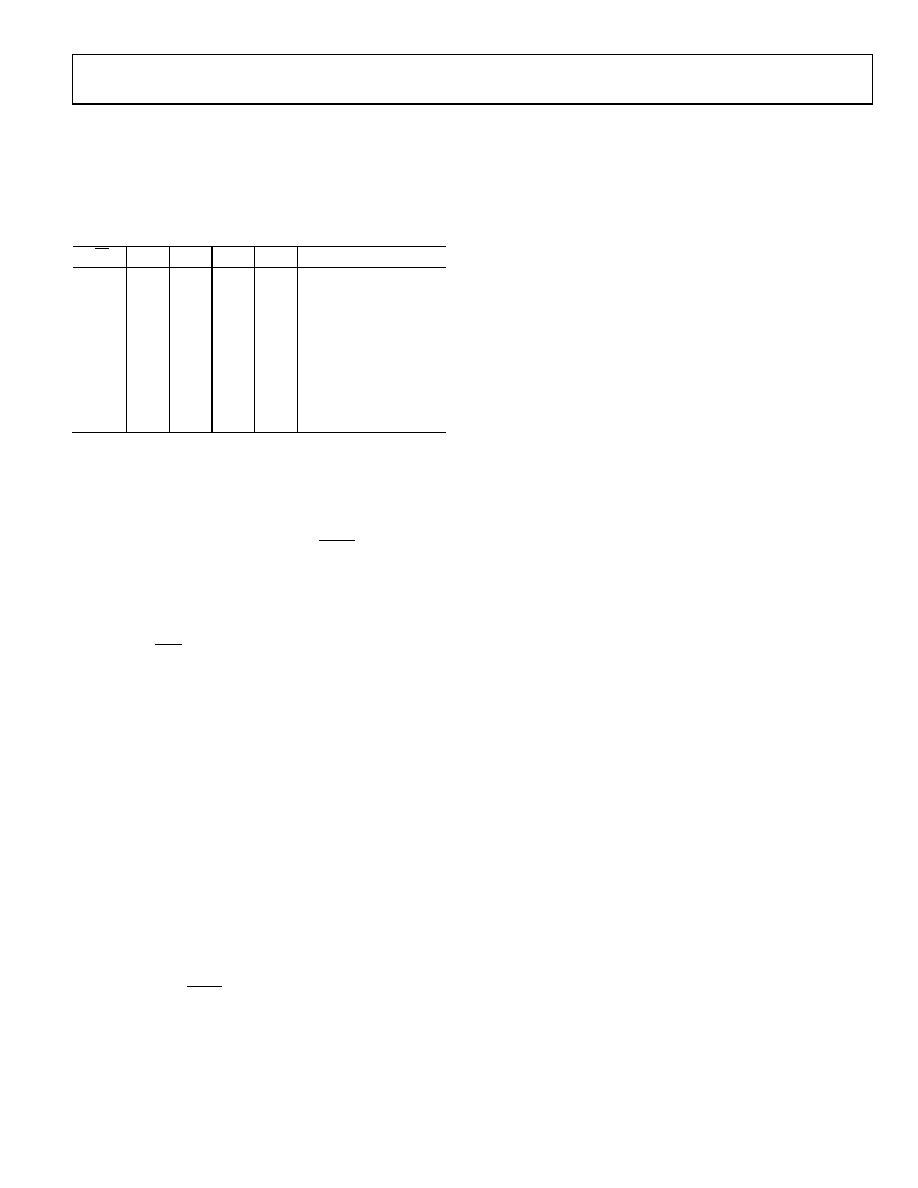
Table 22. SFR Register Functions (REG1 = 0, REG0 = 0)
R/ W
A3
A2
A1
A0
Function
X
0
NOP (no operation)
0
1
Write CLR code
0
1
0
Soft CLR
0
1
0
Soft power-down
0
1
0
1
Soft power-up
0
1
0
Control register write
1
0
Control register read
0
1
0
1
0
Monitor channel
0
1
Soft reset
SFR Commands
NOP (No Operation)
REG1 = REG0 = 0, A3 to A0 = 0000
Performs no operation, but is useful in readback mode to clock
out data on SDO for diagnostic purposes. BUSY outputs a low
during a NOP operation.
Write CLR Code
REG1 = REG0 = 0, A3 to A0 = 0001
DB13 to DB0 = Contain the CLR data
Bringing the CLR line low or exercising the soft clear function
loads the contents of the DAC registers with the data contained
in the user-configurable CLR register and sets VOUT 0 to
VOUT 15, accordingly. This can be very useful not only for
setting up a specific output voltage in a clear condition but for
calibration purposes. For calibration, the user can load full scale
or zero scale to the clear code register and then issue a hardware
or software clear to load this code to all DACs, removing the
need for individual writes to all DACs. Default on power-up
is all zeros.
Soft CLR
REG1 = REG0 = 0, A3 to A0 = 0010
DB13 to DB0 = Don’t Care
Executing this instruction performs the CLR, which is
functionally the same as that provided by the external CLR pin.
The DAC outputs are loaded with the data in the CLR code
register. The time taken to execute fully the SOFT CLR is
20 s on the AD5390/AD5391 and 15 s on the AD5392. It
is indicated by the BUSY low time.
Soft Power-Down
REG1 = REG0 = 0, A3 to A0 = 1000
DB13 to DB0 = Don’t Care
Executing this instruction performs a global power-down,
which puts all channels into a low power mode, reducing analog
current to 1 A maximum and digital power consumption to
20 A maximum. In power-down mode, the output amplifier
can be configured as a high impedance output or can provide a
100 k load to ground. The contents of all internal registers are
retained in power-down mode.
Soft Power-Up
REG1 = REG0 = 0, A3 to A0 =1001
DB13 to DB0 = Don’t Care
This instruction is used to power up the output amplifiers and
the internal references. The time to exit power-down mode is
8 s. The hardware power-down and software functions are
internally combined in a digital OR function.
Soft Reset
REG1 = REG0 = 0, A5 to A0 = 001111
DB13 to DB0 = Don’t Care
This instruction is used to implement a software reset. All
internal registers are reset to their default values, which
correspond to m at full scale and c at zero scale. The contents
of the DAC registers are cleared, setting all analog outputs to
0 V. The soft reset activation time is 135 s maximum.
Monitor Channel
REG1 = REG0 = 0, A3 to A0 = 01010
DB13 to DB8 = Contain data to address the channel to be
monitored
A monitor function is provided on all devices. This feature,
consisting of a multiplexer addressed via the interface, allows
any channel output to be routed to the MON_OUT pin for
monitoring using an external ADC. In addition to monitoring
all output channels, two external inputs are also provided,
allowing the user to monitor signals external to the AD539x.
The channel monitor function must be enabled in the control
register before any channels are routed to the MON_OUT pin.
On the AD5390 and AD5392 14-bit parts, DB13 to DB8 contain
the channel address for the monitored channel. On the AD5391
12-bit part, DB11 to DB6 contain the channel address for the
channel to be monitored. Selecting Address 63 three-states the
MON_OUT pin.
The channel monitor decoding for the AD5390/AD5392 is
shown in Table 23 and the monitor decoding for the AD5391 is
shown in Table 24.
相关PDF资料 |
PDF描述 |
|---|---|
| MS27473T20B35PLC | CONN HSG PLUG 79POS STRGHT PIN |
| VE-2WP-MY-F1 | CONVERTER MOD DC/DC 13.8V 50W |
| AD669ARZ | IC DAC 16BIT MONO W/VREF 28-SOIC |
| VI-BW0-MV-F2 | CONVERTER MOD DC/DC 5V 150W |
| MS27496E23F53S | CONN RCPT 53POS BOX MNT W/SCKT |
相关代理商/技术参数 |
参数描述 |
|---|---|
| AD5398ABCBZ-REEL | 功能描述:IC DAC 10BIT CURRENT-SINK 9WLCSP RoHS:是 类别:集成电路 (IC) >> 数据采集 - 数模转换器 系列:- 产品培训模块:Data Converter Fundamentals DAC Architectures 设计资源:Unipolar, Precision DC Digital-to-Analog Conversion using AD5450/1/2/3 8-14-Bit DACs (CN0052) Precision, Bipolar, Configuration for AD5450/1/2/3 8-14bit Multiplying DACs (CN0053) AC Signal Processing Using AD5450/1/2/3 Current Output DACs (CN0054) Programmable Gain Element Using AD5450/1/2/3 Current Output DAC Family (CN0055) Single Supply Low Noise LED Current Source Driver Using a Current Output DAC in the Reverse Mode (CN0139) 标准包装:10,000 系列:- 设置时间:- 位数:12 数据接口:DSP,MICROWIRE?,QSPI?,串行,SPI? 转换器数目:1 电压电源:单电源 功率耗散(最大):- 工作温度:-40°C ~ 125°C 安装类型:表面贴装 封装/外壳:SOT-23-8 薄型,TSOT-23-8 供应商设备封装:TSOT-23-8 包装:带卷 (TR) 输出数目和类型:1 电流,单极;1 电流,双极 采样率(每秒):2.7M |
| AD5398ABCBZ-REEL7 | 功能描述:IC DAC 10BIT CURRENT-SINK 9WLCSP RoHS:是 类别:集成电路 (IC) >> 数据采集 - 数模转换器 系列:- 产品培训模块:Lead (SnPb) Finish for COTS Obsolescence Mitigation Program 标准包装:50 系列:- 设置时间:4µs 位数:12 数据接口:串行 转换器数目:2 电压电源:单电源 功率耗散(最大):- 工作温度:-40°C ~ 85°C 安装类型:表面贴装 封装/外壳:8-TSSOP,8-MSOP(0.118",3.00mm 宽) 供应商设备封装:8-uMAX 包装:管件 输出数目和类型:2 电压,单极 采样率(每秒):* 产品目录页面:1398 (CN2011-ZH PDF) |
| AD5398A-WAFER | 功能描述:10 Bit Digital to Analog Converter 1 9-WLCSP (1.52 x 1.69) 制造商:analog devices inc. 系列:- 包装:散装 零件状态:上次购买时间 位数:10 数模转换器数:1 建立时间:250μs(标准) 输出类型:Current - Unbuffered 差分输出:无 数据接口:I2C 参考类型:内部 电压 - 电源,模拟:2.7 V ~ 5.5 V 电压 - 电源,数字:2.7 V ~ 5.5 V INL/DNL(LSB):±1.5,±1(最大) 架构:电流阱 工作温度:-30°C ~ 85°C 封装/外壳:9-UFBGA,WLCSP 供应商器件封装:9-WLCSP(1.52 x 1.69) 标准包装:1 |
| AD5398BCBZ-REEL | 功能描述:IC DAC 10BIT CURRENT-SINK 9WLCSP RoHS:是 类别:集成电路 (IC) >> 数据采集 - 数模转换器 系列:- 标准包装:2,400 系列:- 设置时间:- 位数:18 数据接口:串行 转换器数目:3 电压电源:模拟和数字 功率耗散(最大):- 工作温度:-40°C ~ 85°C 安装类型:表面贴装 封装/外壳:36-TFBGA 供应商设备封装:36-TFBGA 包装:带卷 (TR) 输出数目和类型:* 采样率(每秒):* |
| AD5398BCBZ-REEL7 | 功能描述:IC DAC 10BIT CURRENT-SINK 9WLCSP RoHS:是 类别:集成电路 (IC) >> 数据采集 - 数模转换器 系列:- 产品培训模块:Lead (SnPb) Finish for COTS Obsolescence Mitigation Program 标准包装:50 系列:- 设置时间:4µs 位数:12 数据接口:串行 转换器数目:2 电压电源:单电源 功率耗散(最大):- 工作温度:-40°C ~ 85°C 安装类型:表面贴装 封装/外壳:8-TSSOP,8-MSOP(0.118",3.00mm 宽) 供应商设备封装:8-uMAX 包装:管件 输出数目和类型:2 电压,单极 采样率(每秒):* 产品目录页面:1398 (CN2011-ZH PDF) |
发布紧急采购,3分钟左右您将得到回复。