参数资料
| 型号: | AD5590BBC |
| 厂商: | Analog Devices Inc |
| 文件页数: | 20/44页 |
| 文件大小: | 0K |
| 描述: | IC ADC I/O PORT16 W/AMP 80CSPBGA |
| 标准包装: | 1 |
| 位数: | 12 |
| 采样率(每秒): | 1M |
| 数据接口: | DSP,MICROWIRE?,QSPI?,串行,SPI? |
| 转换器数目: | 2 |
| 功率耗散(最大): | 12.5mW |
| 电压电源: | 单电源 |
| 工作温度: | -40°C ~ 85°C |
| 安装类型: | 表面贴装 |
| 封装/外壳: | 80-LFBGA,CSPBGA |
| 供应商设备封装: | 80-CSP-BGA(10x10) |
| 包装: | 托盘 |
| 输入数目和类型: | 16 个单端,单极 |
第1页第2页第3页第4页第5页第6页第7页第8页第9页第10页第11页第12页第13页第14页第15页第16页第17页第18页第19页当前第20页第21页第22页第23页第24页第25页第26页第27页第28页第29页第30页第31页第32页第33页第34页第35页第36页第37页第38页第39页第40页第41页第42页第43页第44页
AD5590
Rev. A | Page 27 of 44
ADC SECTION
The ADC section is a fast, 16-channel, 12-bit, single-supply,
analog-to-digital converter. The ADC is capable of throughput
rates of up to 1 MSPS when provided with a 20 MHz clock.
The ADC section provides the user with an on-chip track-
and-hold, analog-to-digital converter. The ADC section has
16 single-ended input channels with a channel sequencer,
allowing the user to select a sequence of channels through
which the ADC can cycle with each consecutive ASYNC falling
edge. The serial clock input accesses data from the ADC, controls
the transfer of data written to the ADC, and provides the clock
source for the successive approximation ADC converter. The
analog input range for the ADC is 0 V to VREFA or 0 V to 2 ×
VREFA depending on the status of Bit 1 in the control register.
The ADC provides flexible power management options to
allow the user to achieve the best power performance for a
given throughput rate. These options are selected by program-
ming the power management bits in the ADC control register.
ADC CONVERTER OPERATION
The ADC is a 12-bit successive approximation analog-to-digital
converter based around a capacitive DAC. The ADC can convert
analog input signals in the range 0 V to VREFA or 0 V to 2 × VREFA.
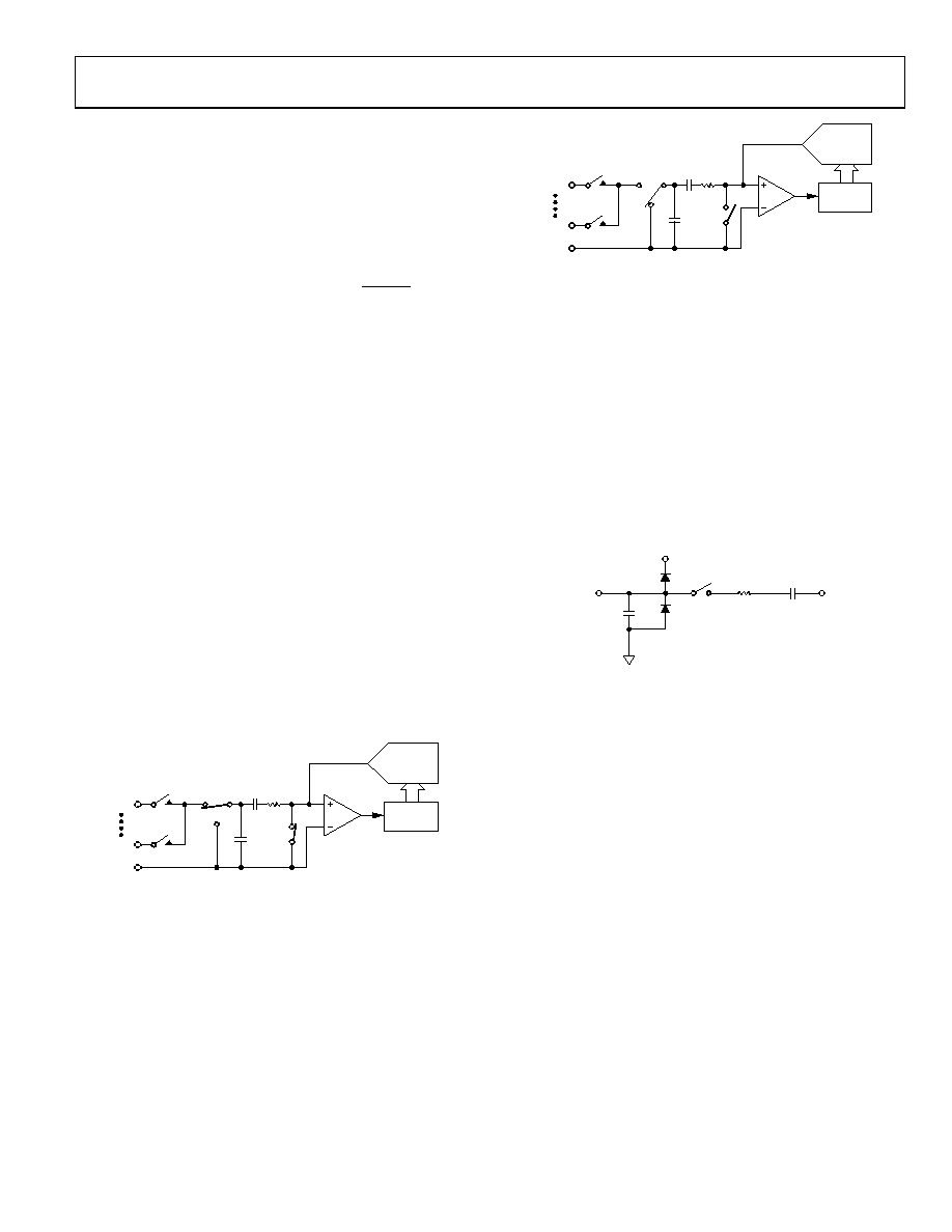
Figure 54 and Figure 55 show simplified schematics of the ADC.
The ADC comprises control logic, SAR, and a capacitive DAC,
which are used to add and subtract fixed amounts of charge
from the sampling capacitor to bring the comparator back
into a balanced condition. Figure 54 shows the ADC during
its acquisition phase. SW2 is closed and SW1 is in Position
A. The comparator is held in a balanced condition and the
sampling capacitor acquires the signal on the selected VIN
channel.
VIN0
VIN15
ADCGND
A
B
SW1
SW2
4k
COMPARATOR
CAPACITIVE
DAC
CONTROL
LOGIC
07691-
054
Figure 54. ADC Acquisition Phase
When the ADC starts a conversion (see Figure 55), SW2 opens
and SW1 moves to Position B, causing the comparator to become
unbalanced. The control logic and the capacitive DAC are used
to add and subtract fixed amounts of charge from the sampling
capacitor to bring the comparator back into a balanced condi-
tion. When the comparator is rebalanced, the conversion is
complete. The control logic generates the ADC output code.
Figure 57 shows the ADC transfer function.
VIN0
VIN15
ADCGND
A
B
SW1
SW2
4k
COMPARATOR
CAPACITIVE
DAC
CONTROL
LOGIC
07691-
055
Figure 55. ADC Conversion Phase
Analog Input
Figure 56 shows an equivalent circuit of the analog input structure
of the ADC. The two diodes, D1 and D2, provide ESD protection
for the analog inputs. Care must be taken to ensure that the analog
input signal never exceed the supply rails by more than 200 mV.
This causes these diodes to become forward biased and start
conducting current into the substrate. 10 mA is the maximum
current these diodes can conduct without causing irreversible
damage to the ADC. Capacitor C1 in Figure 56 is typically about
4 pF and can primarily be attributed to pin capacitance. Resistor
R1 is a lumped component made up of the on resistance of a
switch (track-and-hold switch) and also includes the on resis-
tance of the input multiplexer.
C1
4pF
VINx
CONVERSION PHASE—SWITCH OPEN
TRACK PHASE—SWITCH CLOSED
ADCVDD
R1
C2
30pF
D2
D1
07691-
056
Figure 56. Equivalent Analog Input Circuit
The total resistance is typically about 400 . Capacitor C2 is
the ADC sampling capacitor and typically has a capacitance of
30 pF. For ac applications, removing high frequency components
from the analog input signal is recommended by use of an RC
low-pass filter on the relevant analog input pin. In applications
where harmonic distortion and signal-to-noise ratio are critical,
drive the analog input from a low impedance source. Large
source impedances significantly affect the ac performance of
the ADC. This may necessitate the use of an input buffer
amplifier. The choice of the op amp is a function of the
particular application.
When no amplifier is used to drive the analog input, limit the
source impedance to low values. The maximum source impedance
depends on the amount of total harmonic distortion (THD) that
can be tolerated. The THD increases as the source impedance
increases, and performance degrades (see Figure 28).
相关PDF资料 |
PDF描述 |
|---|---|
| AD5621BKSZ-500RL7 | IC DAC 12BIT SPI 5V SC70-6 |
| AD5626BRMZ-REEL7 | IC DAC NANO 12BIT 8-MSOP |
| AD5662BRM-1 | IC DAC 16BIT BUFF V-OUT 8-MSOP |
| AD5663RBCPZ-3R2 | IC DAC NANO 16BIT DUAL 10-LFCSP |
| AD5664BCPZ-R2 | IC DAC NANO 16BIT QUAD 10-LFCSP |
相关代理商/技术参数 |
参数描述 |
|---|---|
| AD5590BBCZ | 功能描述:IC ADC I/O PORT-16 AMP 80-CSPBGA RoHS:是 类别:集成电路 (IC) >> 数据采集 - 模数转换器 系列:- 其它有关文件:TSA1204 View All Specifications 标准包装:1 系列:- 位数:12 采样率(每秒):20M 数据接口:并联 转换器数目:2 功率耗散(最大):155mW 电压电源:模拟和数字 工作温度:-40°C ~ 85°C 安装类型:表面贴装 封装/外壳:48-TQFP 供应商设备封装:48-TQFP(7x7) 包装:Digi-Reel® 输入数目和类型:4 个单端,单极;2 个差分,单极 产品目录页面:1156 (CN2011-ZH PDF) 其它名称:497-5435-6 |
| AD5592RBCBZ-1-RL7 | 功能描述:IC DAC/ADC 12BIT OCT SPI 16WLCSP 制造商:analog devices inc. 系列:- 包装:剪切带(CT) 零件状态:在售 类型:ADC,DAC 分辨率(位):12 b 采样率(每秒):400k 数据接口:SPI 电压源:单电源 电压 - 电源:2.7 V ~ 5.5 V 工作温度:-40°C ~ 105°C 安装类型:表面贴装 封装/外壳:16-UFBGA,WLCSP 供应商器件封装:16-WLCSP(1.96x1.96) 标准包装:1 |
| AD5592RBCBZ-RL7 | 功能描述:IC DAC/ADC 12BIT OCT SPI 16WLCSP 制造商:analog devices inc. 系列:* 零件状态:在售 标准包装:1 |
| AD5592RBCPZ-1-RL7 | 功能描述:IC DAC/ADC 12BIT OCT SPI 16LFCSP 制造商:analog devices inc. 系列:* 零件状态:在售 标准包装:1 |
| AD5592RBCPZ-RL7 | 功能描述:IC DAC/ADC 12BIT OCT SPI 16LFCSP 制造商:analog devices inc. 系列:- 包装:剪切带(CT) 零件状态:在售 类型:ADC,DAC 分辨率(位):12 b 采样率(每秒):400k 数据接口:SPI 电压源:单电源 电压 - 电源:2.7 V ~ 5.5 V 工作温度:-40°C ~ 105°C 安装类型:表面贴装 封装/外壳:16-WFQFN,CSP 供应商器件封装:16-LFCSP-WQ(3x3) 标准包装:1 |
发布紧急采购,3分钟左右您将得到回复。