参数资料
| 型号: | AD5749ACPZ-RL7 |
| 厂商: | Analog Devices Inc |
| 文件页数: | 1/28页 |
| 文件大小: | 0K |
| 描述: | IC CURRENT OUT DVR 32-LFCSP |
| 标准包装: | 1 |
| 放大器类型: | 仪表 |
| 电路数: | 1 |
| 电流 - 电源: | 5.2mA |
| 电流 - 输出 / 通道: | 24mA |
| 电压 - 电源,单路/双路(±): | 10.8 V ~ 55 V |
| 工作温度: | -40°C ~ 105°C |
| 安装类型: | 表面贴装 |
| 封装/外壳: | 32-VFQFN 裸露焊盘,CSP |
| 供应商设备封装: | 32-LFCSP-VQ(5x5) |
| 包装: | 标准包装 |
| 其它名称: | AD5749ACPZ-RL7DKR |
当前第1页第2页第3页第4页第5页第6页第7页第8页第9页第10页第11页第12页第13页第14页第15页第16页第17页第18页第19页第20页第21页第22页第23页第24页第25页第26页第27页第28页
Industrial Current Out Driver, Single-Supply,
55 V Maximum Supply, Programmable Ranges
Data Sheet
Rev. B
Information furnished by Analog Devices is believed to be accurate and reliable. However, no
responsibilityisassumedbyAnalogDevicesforitsuse,norforanyinfringementsofpatentsorother
rightsofthirdpartiesthatmayresultfromitsuse.Specificationssubjecttochangewithoutnotice.No
license is granted by implication or otherwise under any patent or patent rights of Analog Devices.
Trademarksandregisteredtrademarksarethepropertyoftheirrespectiveowners.
One Technology Way, P.O. Box 9106, Norwood, MA 02062-9106, U.S.A.
Tel: 781.329.4700
2010–2013 Analog Devices, Inc. All rights reserved.
FEATURES
Current output ranges: 0 mA to 24 mA or 4 mA to 20 mA
±0.03% FSR typical total unadjusted error (TUE)
±5 ppm/°C typical output drift
2% overrange
Flexible serial digital interface
On-chip output fault detection
PEC error checking
Asynchronous CLEAR function
Power supply range
AVDD: 12 V (± 10%) to 55 V (maximum)
Output loop compliance to AVDD 2.75 V
Temperature range: 40°C to +105°C
32-lead, 5 mm × 5 mm LFCSP package
APPLICATIONS
Process control
Actuator control
PLCs
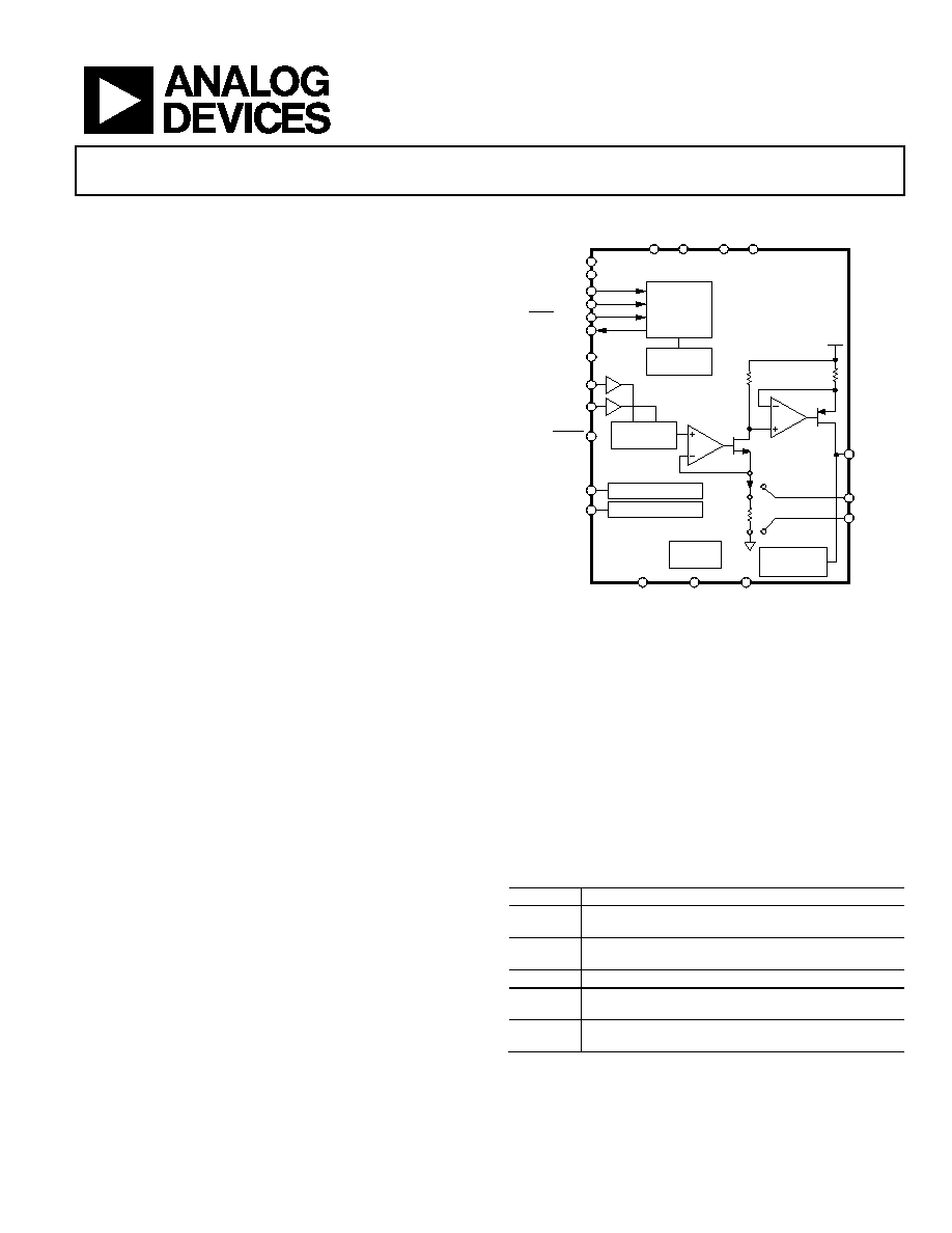
FUNCTIONAL BLOCK DIAGRAM
Figure 1.
GENERAL DESCRIPTION
The AD5749 is a single channel, low cost, precision, current output
driver with hardware or software programmable output ranges.
The software ranges are configured via an SPI-/MICROWIRE-
compatible serial interface. The AD5749 targets applications in
PLC and industrial process control. The analog input to the
AD5749 is provided from a low voltage, single-supply digital-to-
analog converter (DAC) and is internally conditioned to provide
the desired output current/voltage range.
The output current range is programmable across two current
ranges: 0 mA to 24 mA, or 4 mA to 20 mA. Current output is
open-circuit protected and can drive inductive loads of 0.1 H.
The device is specified to operate with a power supply range
from 10.8 V to 55 V. Output loop compliance is 0 V to AVDD
2.75 V.
The flexible serial interface is SPI and MICROWIRE compatible
and can be operated in 3-wire mode to minimize the digital
isolation required in isolated applications. The interface also
features an optional PEC error checking feature using CRC-8
error checking, useful in industrial environments where data
communication corruption can occur.
The device also includes a power-on reset function ensuring
that the device powers up in a known state and an asynchron-
ous CLEAR pin that sets the outputs to the low end of the
selected current range.
An HW SELECT pin is used to configure the part for hardware
or software mode on power-up.
Table 1. Related Devices
Part No.
Description
Industrial current/voltage output (I/V) driver with
programmable ranges
Industrial I/V output driver, single-supply, 55 V maximum
supply, programmable ranges
Industrial I/V output driver with programmable ranges
Single-channel, 12-/16-bit, serial input, current source
output DAC
Single-channel, 12-/16-bit, serial input, I/V output DAC
08923-
001
*DENOTES SHARED PIN. SOFTWARE MODE DENOTED BY REGULAR TEXT,
HARDWARE MODE DENOTED BY ITALIC TEXT. FOR EXAMPLE, FOR
FAULT/TEMP PIN, IN SOFTWARE MODE, THIS PIN TAKES ON FAULT
FUNCTION. IN HARDWARE MODE, THIS PIN TAKES ON TEMP FUNCTION.
CLEAR
DVCC GND
AVDD GND
CLRSEL
HW SELECT
VIN
VREF
OVERTEMP
IOUT OPEN FAULT
RESET
R2
RSET
AVDD
R3
AD5749
IOUT
POWER-
ON RESET
IOUT
OPEN FAULT
IOUT RANGE
SCALING
STATUS
REGISTER
INPUT SHIFT
REGISTER
AND
CONTROL
LOGIC
SCLK/OUTEN*
SDIN/R0*
SYNC/RSET*
SDO/VFAULT*
FAULT/TEMP*
NC/IFAULT*
AD2/R1*
AD1/R2*
AD0/R3*
REXT1
REXT2
相关PDF资料 |
PDF描述 |
|---|---|
| NPPC192KFMS-RC | CONN FMALE 38POS DL .1" GOLD SMD |
| 2-1879208-5 | RES 100 OHM 1/16W 0.1% 0402 |
| 0001.2522 | FUSE 630MA 250V 6.3X32 T-LAG |
| 0001.2523 | FUSE 800MA 250V 6.3X32 T-LAG |
| 0001.2524 | FUSE 1A 250V 6.3X32 T-LAG |
相关代理商/技术参数 |
参数描述 |
|---|---|
| AD574A | 制造商:AD 制造商全称:Analog Devices 功能描述:Complete 12-Bit A/D Converter |
| AD574AJ | 制造商:AD 制造商全称:Analog Devices 功能描述:Complete 12-Bit A/D Converter |
| AD574AJD | 功能描述:IC ADC 12BIT W/REF 28-CDIP RoHS:否 类别:集成电路 (IC) >> 数据采集 - 模数转换器 系列:- 标准包装:1 系列:- 位数:14 采样率(每秒):83k 数据接口:串行,并联 转换器数目:1 功率耗散(最大):95mW 电压电源:双 ± 工作温度:0°C ~ 70°C 安装类型:通孔 封装/外壳:28-DIP(0.600",15.24mm) 供应商设备封装:28-PDIP 包装:管件 输入数目和类型:1 个单端,双极 |
| AD574AJD/+ | 制造商:Analog Devices 功能描述:ADC SGL SAR 12-BIT PARALLEL 28PIN SBDIP - Rail/Tube 制造商:Rochester Electronics LLC 功能描述:IC, MONO 12-BIT A/D CONV - Bulk |
发布紧急采购,3分钟左右您将得到回复。