参数资料
| 型号: | AD5749ACPZ-RL7 |
| 厂商: | Analog Devices Inc |
| 文件页数: | 18/28页 |
| 文件大小: | 0K |
| 描述: | IC CURRENT OUT DVR 32-LFCSP |
| 标准包装: | 1 |
| 放大器类型: | 仪表 |
| 电路数: | 1 |
| 电流 - 电源: | 5.2mA |
| 电流 - 输出 / 通道: | 24mA |
| 电压 - 电源,单路/双路(±): | 10.8 V ~ 55 V |
| 工作温度: | -40°C ~ 105°C |
| 安装类型: | 表面贴装 |
| 封装/外壳: | 32-VFQFN 裸露焊盘,CSP |
| 供应商设备封装: | 32-LFCSP-VQ(5x5) |
| 包装: | 标准包装 |
| 其它名称: | AD5749ACPZ-RL7DKR |
第1页第2页第3页第4页第5页第6页第7页第8页第9页第10页第11页第12页第13页第14页第15页第16页第17页当前第18页第19页第20页第21页第22页第23页第24页第25页第26页第27页第28页
Data Sheet
AD5749
Rev. B | Page 25 of 28
LAYOUT GUIDELINES
In any circuit where accuracy is important, careful consideration
of the power supply and ground return layout helps to ensure
the rated performance. The PCB on which the AD5749 is
mounted should be designed so that the AD5749 lies on the
analog plane.
The AD5749 should have ample supply bypassing of 10 F in
parallel with 0.1 F on each supply, located as close to the
package as possible, ideally right up against the device. The
10 F capacitors are the tantalum bead type. The 0.1 F capaci-
tor should have low effective series resistance (ESR) and low
effective series inductance (ESI) such as the common ceramic
types, which provide a low impedance path to ground at high
frequencies to handle transient currents due to internal logic
switching.
In systems where there are many devices on one board, it is often
useful to provide some heat sinking capability to allow the power
to dissipate easily.
Figure 36. Paddle Connection to Board
The AD5749 has an exposed paddle beneath the device.
Connect this paddle to the GND of the AD5749. For optimum
performance, special considerations should be used to design
the motherboard and to mount the package. For enhanced
thermal, electrical, and board level performance, the exposed
paddle on the bottom of the package should be soldered to the
corresponding thermal land paddle on the PCB (GND).
Thermal vias should be designed into the PCB land paddle area
to further improve heat dissipation.
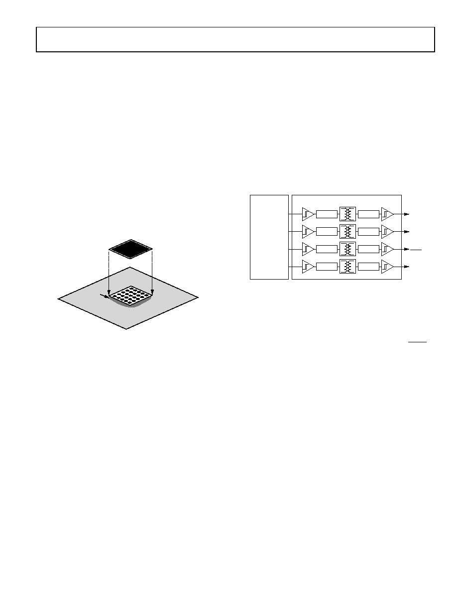
GALVANICALLY ISOLATED INTERFACE
In many process control applications, it is necessary to provide
an isolation barrier between the controller and the unit being
controlled to protect and isolate the controlling circuitry from
any hazardous common-mode voltages that may occur. The
iCoupler family of products from Analog Devices, Inc., provides
voltage isolation in excess of 5.0 kV. The serial loading structure
of the AD5749 makes it ideal for isolated interfaces because the
number of interface lines is kept to a minimum. Figure 37 shows a
4-channel isolated interface to the AD5749 using an ADuM1400.
For further information, visit http://www.analog.com/icouplers.
Figure 37. Isolated Interface
MICROPROCESSOR INTERFACING
Microprocessor interfacing to the AD5749 is via a serial bus that
uses a protocol compatible with microcontrollers and DSP proces-
sors. The communication channel is a 3-wire (minimum)
interface consisting of a clock signal, a data signal, and a SYNC
signal. The AD5749 requires a 16-bit data-word with data valid
on the falling edge of SCLK.
AD5749
GND
PLANE
BOARD
08923-
037
VIA
VOA
VIB
VOB
VIC
VOC
VID
VOD
ENCODE
DECODE
ENCODE
DECODE
ENCODE
DECODE
ENCODE
DECODE
08923-
038
SERIAL
CLOCK OUT
SERIAL
DATA OUT
SYNC OUT
CONTROL OUT
CONTROLLER
TO
SCLK
TO
SDIN
TO
SYNC
TO
CLEAR
ADuM14001
1ADDITIONAL PINS OMITTED FOR CLARITY.
相关PDF资料 |
PDF描述 |
|---|---|
| NPPC192KFMS-RC | CONN FMALE 38POS DL .1" GOLD SMD |
| 2-1879208-5 | RES 100 OHM 1/16W 0.1% 0402 |
| 0001.2522 | FUSE 630MA 250V 6.3X32 T-LAG |
| 0001.2523 | FUSE 800MA 250V 6.3X32 T-LAG |
| 0001.2524 | FUSE 1A 250V 6.3X32 T-LAG |
相关代理商/技术参数 |
参数描述 |
|---|---|
| AD574A | 制造商:AD 制造商全称:Analog Devices 功能描述:Complete 12-Bit A/D Converter |
| AD574AJ | 制造商:AD 制造商全称:Analog Devices 功能描述:Complete 12-Bit A/D Converter |
| AD574AJD | 功能描述:IC ADC 12BIT W/REF 28-CDIP RoHS:否 类别:集成电路 (IC) >> 数据采集 - 模数转换器 系列:- 标准包装:1 系列:- 位数:14 采样率(每秒):83k 数据接口:串行,并联 转换器数目:1 功率耗散(最大):95mW 电压电源:双 ± 工作温度:0°C ~ 70°C 安装类型:通孔 封装/外壳:28-DIP(0.600",15.24mm) 供应商设备封装:28-PDIP 包装:管件 输入数目和类型:1 个单端,双极 |
| AD574AJD/+ | 制造商:Analog Devices 功能描述:ADC SGL SAR 12-BIT PARALLEL 28PIN SBDIP - Rail/Tube 制造商:Rochester Electronics LLC 功能描述:IC, MONO 12-BIT A/D CONV - Bulk |
发布紧急采购,3分钟左右您将得到回复。