参数资料
| 型号: | AD5749ACPZ-RL7 |
| 厂商: | Analog Devices Inc |
| 文件页数: | 14/28页 |
| 文件大小: | 0K |
| 描述: | IC CURRENT OUT DVR 32-LFCSP |
| 标准包装: | 1 |
| 放大器类型: | 仪表 |
| 电路数: | 1 |
| 电流 - 电源: | 5.2mA |
| 电流 - 输出 / 通道: | 24mA |
| 电压 - 电源,单路/双路(±): | 10.8 V ~ 55 V |
| 工作温度: | -40°C ~ 105°C |
| 安装类型: | 表面贴装 |
| 封装/外壳: | 32-VFQFN 裸露焊盘,CSP |
| 供应商设备封装: | 32-LFCSP-VQ(5x5) |
| 包装: | 标准包装 |
| 其它名称: | AD5749ACPZ-RL7DKR |
第1页第2页第3页第4页第5页第6页第7页第8页第9页第10页第11页第12页第13页当前第14页第15页第16页第17页第18页第19页第20页第21页第22页第23页第24页第25页第26页第27页第28页
Data Sheet
AD5749
Rev. B | Page 21 of 28
Status Bit Read Operation
A read of the status bits can be initiated as part of a normal write
operation. The read is activated by selecting the correct device
address (A2, A1, A0) and then setting the R/W bit to 1. By
default, the SDO pin is disabled. After having addressed the
AD5749 and setting R/W to 1 the SDO pin is enabled and data
is clocked out on the 5th rising edge of SCLK. After all the data
has been clocked out on SDO, a rising edge on SYNC disables
(tristates) the SDO pin again. Status register data (see Table 9)
and control register data are both available during the same
read cycle. Data contained in Bit D10 to Bit D0 of the write
operation are still valid and can be used to change the operating
mode of the AD5749 if required.
The status bits comprise three read-only bits. They are used to
notify the user of specific fault conditions that occur, such as
an open circuit on the output, over-temperature error or an
interface error. If any of these fault conditions occur, a hardware
FAULT is also asserted low, which can be used as a hardware
interrupt to the controller.
See the Detailed Description of Features section for a full
explanation of fault conditions.
HARDWARE CONTROL
Hardware control is enabled by connecting the HW SELECT
pin to DVCC. In this mode, the R3, R2, R1, and R0 pins, in
conjunction with the RSET pin, are used to configure the
output range, as per Table 8.
In hardware mode, there is no status register. The fault conditions
(open circuit, and overtemperature) are available on Pin IFAULT
and Pin TEMP. If any one of these fault conditions is set, a low is
asserted on the specific fault pin. IFAULT and TEMP are open-
drain outputs and, therefore, can be connected together to allow the
user to generate one interrupt to the system controller to commun-
icate a fault. If hardwired in this way, it is not possible to isolate
which fault occurred in the system.
TRANSFER FUNCTION
The AD5749 consists of an internal signal conditioning block
that maps the analog input voltage to a programmed output
range. The available analog input range is 0 V to 4.096 V.
For all ranges, the AD5749 implements a straight linear
mapping function, where 0 V maps to the lower end of the
selected range and 4.096 V maps to the upper end of the
selected range.
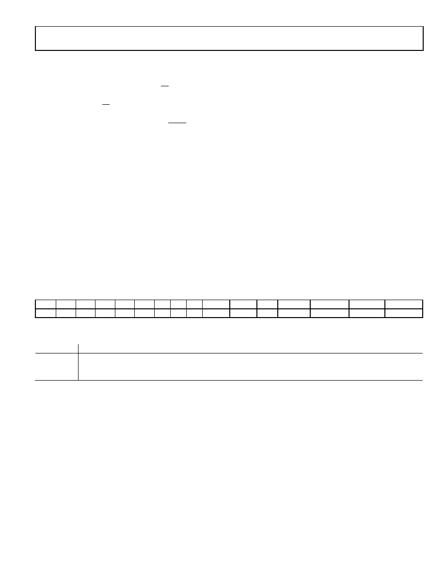
Table 9. Input Shift Register Contents for a Read Operation—Status Register
MSB
LSB
D15
D14
D13
D12
D11
D10
D9
D8
D7
D6
D5
D4
D3
D2
D1
D0
A2
A1
A0
1
0
R3
R2
R1
R0
CLRSEL
OUTEN
RSET
PEC Error
OVER TEMP
IOUT Fault
Unused
Table 10. Status Bit Options
Bit
Description
PEC Error
This bit is set if there is an interface error detected by CRC-8 error checking. See the Detailed Description of Features section.
OVER TEMP
This bit is set if the AD5749 core temperature exceeds approximately 150°C.
IOUT Fault
This bit is set if there is an open circuit on the IOUT pin.
相关PDF资料 |
PDF描述 |
|---|---|
| NPPC192KFMS-RC | CONN FMALE 38POS DL .1" GOLD SMD |
| 2-1879208-5 | RES 100 OHM 1/16W 0.1% 0402 |
| 0001.2522 | FUSE 630MA 250V 6.3X32 T-LAG |
| 0001.2523 | FUSE 800MA 250V 6.3X32 T-LAG |
| 0001.2524 | FUSE 1A 250V 6.3X32 T-LAG |
相关代理商/技术参数 |
参数描述 |
|---|---|
| AD574A | 制造商:AD 制造商全称:Analog Devices 功能描述:Complete 12-Bit A/D Converter |
| AD574AJ | 制造商:AD 制造商全称:Analog Devices 功能描述:Complete 12-Bit A/D Converter |
| AD574AJD | 功能描述:IC ADC 12BIT W/REF 28-CDIP RoHS:否 类别:集成电路 (IC) >> 数据采集 - 模数转换器 系列:- 标准包装:1 系列:- 位数:14 采样率(每秒):83k 数据接口:串行,并联 转换器数目:1 功率耗散(最大):95mW 电压电源:双 ± 工作温度:0°C ~ 70°C 安装类型:通孔 封装/外壳:28-DIP(0.600",15.24mm) 供应商设备封装:28-PDIP 包装:管件 输入数目和类型:1 个单端,双极 |
| AD574AJD/+ | 制造商:Analog Devices 功能描述:ADC SGL SAR 12-BIT PARALLEL 28PIN SBDIP - Rail/Tube 制造商:Rochester Electronics LLC 功能描述:IC, MONO 12-BIT A/D CONV - Bulk |
发布紧急采购,3分钟左右您将得到回复。