参数资料
| 型号: | AD5749ACPZ-RL7 |
| 厂商: | Analog Devices Inc |
| 文件页数: | 10/28页 |
| 文件大小: | 0K |
| 描述: | IC CURRENT OUT DVR 32-LFCSP |
| 标准包装: | 1 |
| 放大器类型: | 仪表 |
| 电路数: | 1 |
| 电流 - 电源: | 5.2mA |
| 电流 - 输出 / 通道: | 24mA |
| 电压 - 电源,单路/双路(±): | 10.8 V ~ 55 V |
| 工作温度: | -40°C ~ 105°C |
| 安装类型: | 表面贴装 |
| 封装/外壳: | 32-VFQFN 裸露焊盘,CSP |
| 供应商设备封装: | 32-LFCSP-VQ(5x5) |
| 包装: | 标准包装 |
| 其它名称: | AD5749ACPZ-RL7DKR |
第1页第2页第3页第4页第5页第6页第7页第8页第9页当前第10页第11页第12页第13页第14页第15页第16页第17页第18页第19页第20页第21页第22页第23页第24页第25页第26页第27页第28页
AD5749
Data Sheet
Rev. B | Page 18 of 28
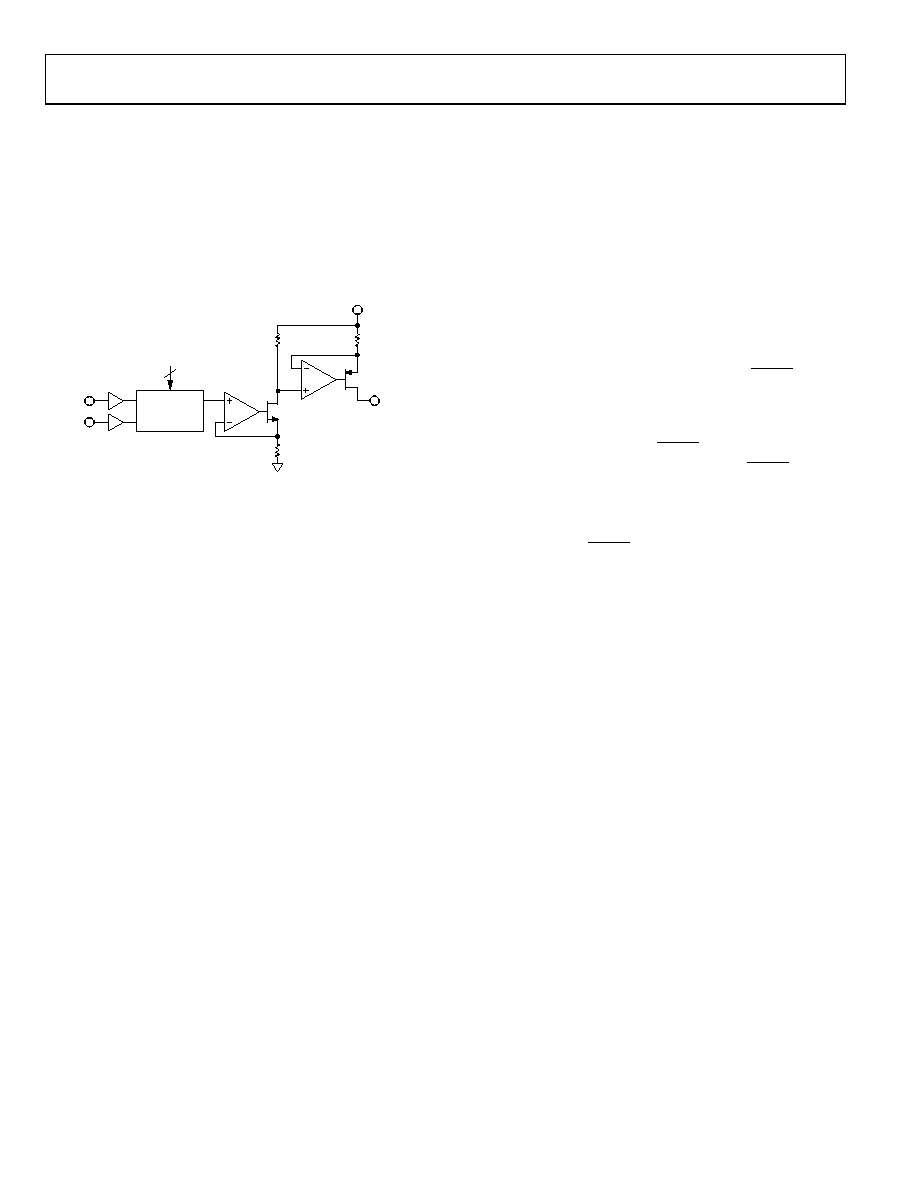
CURRENT OUTPUT ARCHITECTURE
The voltage input from the analog input VIN core (0 V to 4.096 V)
is converted to a current (see Figure 33), which is then mirrored
to the supply rail so that the application simply sees a current
source output with respect to an internal reference voltage. The
reference is used to provide internal offsets for range and gain
scaling. The selectable output range is programmable through
the digital interface (software mode) or via the range pins (R0 to
R3) (hardware mode).
Figure 33. Current Output Configuration
DRIVING INDUCTIVE LOADS
When driving inductive or poorly defined loads, connect a 0.01 F
capacitor between IOUT and GND. This ensures stability with
loads beyond 50 mH. There is no maximum capacitance limit.
The capacitive component of the load may cause slower settling.
POWER-ON STATE OF THE AD5749
On power-up, the AD5749 senses whether hardware or software
mode is loaded and sets the power-up conditions accordingly.
In software SPI mode, the output powers up in the tristate
condition (0 mA).
To put the part into normal operation, the user must set the
OUTEN bit in the control register to enable the output and, in
the same write, set the output range configuration using the R3
to R0 range bits. If the CLEAR pin is still high (active) during
this write, the part automatically clears to its normal clear state
as defined by the programmed range and by the CLRSEL pin or
the CLRSEL bit (see the Asynchronous Clear (CLEAR) section
for more details). The CLEAR pin must be taken low to operate
the part in normal mode.
The CLEAR pin is typically driven directly from a microcontroller.
In cases where the power supply for the AD5749 supply is
independent of the microcontroller power supply, the user can
connect a weak pull-up resistor to DVCC or a pull-down resistor
to ground to ensure that the correct power-up condition is
achieved independent of the microcontroller. A 10 k pull-up/
pull-down resistor on the CLEAR pin should be sufficient for
most applications.
If hardware mode is selected, the part powers up to the conditions
defined by the R3 to R0 range bits and the status of the OUTEN
or CLEAR pin. It is recommended to keep the output disabled
when powering up the part in hardware mode.
DEFAULT REGISTERS AT POWER-ON
The AD5749 power-on-reset circuit ensures that all registers are
loaded with zero code.
In software SPI mode, the part powers up with the output
disabled (OUTEN bit = 0). The user must set the OUTEN bit in
the control register to enable the output and, in the same write,
set the output range configuration using the R3 to R0 bits.
If hardware mode is selected, the part powers up to the
conditions defined by the R3 to R0 bits and the status of the
OUTEN pin. It is recommended to keep the output disabled
when powering up the part in hardware mode.
RESET FUNCTION
In software mode, the part can be reset using the RESET pin
(active low) or the reset bit (reset = 1). A reset disables the
output to its power-on condition. The user must write to the
OUTEN bit to enable the output and, in the same write, set the
output range configuration. The RESET pin is a level sensitive
input; the part stays in reset mode as long as the RESET pin is
low. The reset bit clears to 0 following a reset command to the
control register.
In hardware mode, there is no reset. If using the part in
hardware mode, the RESET pin should be tied high.
OUTEN
In software mode, the output can be enabled or disabled using
the OUTEN bit in the control register. When the output is
disabled, it is placed into tristate. The user must set the OUTEN
bit to enable the output and simultaneously set the output range
configuration.
In hardware mode, the output can be enabled or disabled using
the OUTEN pin. When the output is disabled, it is placed into
tristate. The user must write to the OUTEN pin to enable the
output. It is recommended that the output be disabled when
changing the ranges.
SOFTWARE CONTROL
Software control is enabled by connecting the HW SELECT pin
to ground. In software mode, the AD5749 is controlled over a
versatile 3-wire serial interface that operates at clock rates up to
50 MHz. It is compatible with SPI, QSPI, MICROWIRE, and
DSP standards.
Input Shift Register
The input shift register is 16 bits wide. Data is loaded into the
device MSB first as a 16-bit word under the control of a serial
clock input, SCLK. Data is clocked in on the falling edge of SCLK.
The input shift register consists of 16 control bits, as shown in
Table 7. The timing diagram for this write operation is shown in
Figure 2. The first three bits of the input shift register are used to set
the hardware address of the AD5749 device on the printed circuit
board (PCB). Up to eight devices can be addressed per board.
Bit D11, Bit D1, and Bit D0 must always be set to 0 during any
write sequence.
08923-
034
AVDD
VIN
VREF
A1
A2
R1
R3
R2
T1
T2
RANGE DECODE
FROM INTERFACE
RANGE
SCALING
IOUT
相关PDF资料 |
PDF描述 |
|---|---|
| NPPC192KFMS-RC | CONN FMALE 38POS DL .1" GOLD SMD |
| 2-1879208-5 | RES 100 OHM 1/16W 0.1% 0402 |
| 0001.2522 | FUSE 630MA 250V 6.3X32 T-LAG |
| 0001.2523 | FUSE 800MA 250V 6.3X32 T-LAG |
| 0001.2524 | FUSE 1A 250V 6.3X32 T-LAG |
相关代理商/技术参数 |
参数描述 |
|---|---|
| AD574A | 制造商:AD 制造商全称:Analog Devices 功能描述:Complete 12-Bit A/D Converter |
| AD574AJ | 制造商:AD 制造商全称:Analog Devices 功能描述:Complete 12-Bit A/D Converter |
| AD574AJD | 功能描述:IC ADC 12BIT W/REF 28-CDIP RoHS:否 类别:集成电路 (IC) >> 数据采集 - 模数转换器 系列:- 标准包装:1 系列:- 位数:14 采样率(每秒):83k 数据接口:串行,并联 转换器数目:1 功率耗散(最大):95mW 电压电源:双 ± 工作温度:0°C ~ 70°C 安装类型:通孔 封装/外壳:28-DIP(0.600",15.24mm) 供应商设备封装:28-PDIP 包装:管件 输入数目和类型:1 个单端,双极 |
| AD574AJD/+ | 制造商:Analog Devices 功能描述:ADC SGL SAR 12-BIT PARALLEL 28PIN SBDIP - Rail/Tube 制造商:Rochester Electronics LLC 功能描述:IC, MONO 12-BIT A/D CONV - Bulk |
发布紧急采购,3分钟左右您将得到回复。