- 您现在的位置:买卖IC网 > PDF目录1891 > AD5930YRUZ-REEL7 (Analog Devices Inc)IC GEN PROG FREQ BURST 20TSSOP PDF资料下载
参数资料
| 型号: | AD5930YRUZ-REEL7 |
| 厂商: | Analog Devices Inc |
| 文件页数: | 9/28页 |
| 文件大小: | 0K |
| 描述: | IC GEN PROG FREQ BURST 20TSSOP |
| 产品培训模块: | Direct Digital Synthesis Tutorial Series (1 of 7): Introduction Direct Digital Synthesizer Tutorial Series (7 of 7): DDS in Action Direct Digital Synthesis Tutorial Series (3 of 7): Angle to Amplitude Converter Direct Digital Synthesis Tutorial Series (6 of 7): SINC Envelope Correction Direct Digital Synthesis Tutorial Series (4 of 7): Digital-to-Analog Converter Direct Digital Synthesis Tutorial Series (2 of 7): The Accumulator |
| 标准包装: | 1,000 |
| 分辨率(位): | 10 b |
| 主 fclk: | 50MHz |
| 调节字宽(位): | 24 b |
| 电源电压: | 2.3 V ~ 5.5 V |
| 工作温度: | -40°C ~ 125°C |
| 安装类型: | 表面贴装 |
| 封装/外壳: | 20-TSSOP(0.173",4.40mm 宽) |
| 供应商设备封装: | 20-TSSOP |
| 包装: | 带卷 (TR) |
第1页第2页第3页第4页第5页第6页第7页第8页当前第9页第10页第11页第12页第13页第14页第15页第16页第17页第18页第19页第20页第21页第22页第23页第24页第25页第26页第27页第28页
Data Sheet
AD5930
Rev. | Page 17 of 28
This is beneficial for applications where the user needs to burst
a frequency for a set period, and then “listen” for a response
before increasing to the next frequency. Note also that the
beginning of each frequency increment is at midscale (Phase 0
Rad). Therefore, the phase of the signal is always known.
To set up the AD5930 in burst mode, the CW/BURST bit (D7)
in the control register must be set to 1. See the Activating and
Controlling the Sweep section for more details about the burst
output mode.
SERIAL INTERFACE
The AD5930 has a standard 3-wire serial interface, which is
compatible with SPI, QSPI, MICROWIRE, and DSP
interface standards.
Data is loaded into the device as a 16-bit word under the
control of a serial clock input, SCLK. The timing diagram for
this operation is given in Figure 4.
The FSYNC input is a level-triggered input that acts as a frame
synchronization and chip enable. Data can only be transferred
into the device when FSYNC is low. To start the serial data
transfer, FSYNC should be taken low, observing the minimum
FSYNC to SCLK falling edge setup time, t7. After FSYNC goes
low, serial data is shifted into the device's input shift register on
the falling edges of SCLK for 16 clock pulses. FSYNC can be
taken high after the 16th falling edge of SCLK, observing the
minimum SCLK falling edge to FSYNC rising edge time, t8.
Alternatively, FSYNC can be kept low for a multiple of 16 SCLK
pulses, and then brought high at the end of the data transfer. In
this way, a continuous stream of 16-bit words can be loaded while
FSYNC is held low. FSYNC should only go high after the 16th
SCLK falling edge of the last word is loaded.
The SCLK can be continuous, or, alternatively, the SCLK can
idle high or low between write operations.
POWERING UP THE AD5930
When the AD5930 is powered up, the part is in an undefined
state, and therefore, must be reset before use. The eight registers
(control and frequency) contain invalid data and need to be set
to a known value by the user. The control register should be the
first register to be programmed, as this sets up the part. Note
that a write to the control register automatically resets the
internal state machines and provides an analog output of
midscale as it provides the same function as the INTERRUPT
pin. Typically, this is followed by a serial loading of all the
required sweep parameters. The DAC output remains at
midscale until a sweep is started using the CTRL pin.
PROGRAMMING THE AD5930
The AD5930 is designed to provide automatic frequency sweeps
when the CTRL pin is triggered. The automatic sweep is
controlled by a set of registers, the addresses of which are given
in Table 5. The function of each register is described in more
detail in the following section.
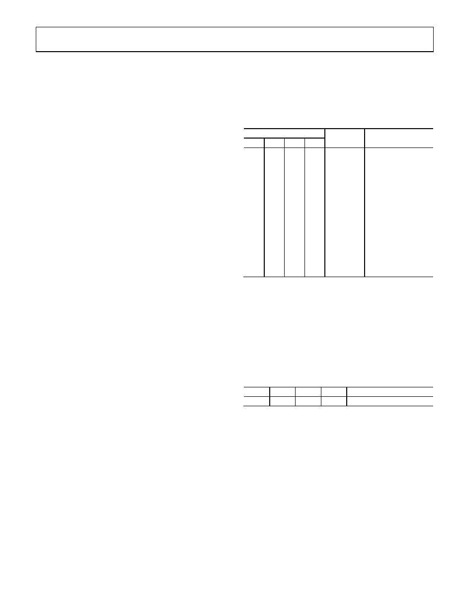
Table 5. Register Addresses
Register Address
D15
D14
D13
D12
Mnemonic
Name
0
CREG
Control bits
0
1
NINCR
Number of
increments
0
1
0
f
Lower 12 bits of delta
frequency
0
1
f
Higher 12 bits of
delta frequency
0
1
tINT
Increment interval
1
0
TBURST
Burst interval
1
0
FSTART
Lower 12 bits of start
frequency
1
0
1
FSTART
Higher 12 bits of start
frequency
1
0
Reserved
1
Reserved
The Control Register
The AD5930 contains a 12-bit control register (see Table 6) that
sets up the operating modes of the AD5930. The different
functions and the various output options from the AD5930 are
controlled by this register.
Table 7 describes the individual bits of the control register.
To address the control register, D15 to D12 of the 16-bit serial
word must be set to 0.
Table 6. Control Register
D15
D14
D13
D12
D11 to D0
0
Control Bits
B
相关PDF资料 |
PDF描述 |
|---|---|
| AD5932YRUZ-REEL7 | IC PROG WAVEFORM GENERAT 16TSSOP |
| AD5933YRSZ-REEL7 | NETWORK ANALYZER 12B 1MSP 16SSOP |
| AD5934YRSZ | IC NTWK ANALYZER 12B 1MSP 16SSOP |
| AD598JR | IC LVDT SGNL COND OSC/REF 20SOIC |
| AD660BR | IC DAC 16BIT MONO W/VREF 24-SOIC |
相关代理商/技术参数 |
参数描述 |
|---|---|
| AD5932 | 制造商:AD 制造商全称:Analog Devices 功能描述:Programmable Frequency Scan Waveform Generator |
| AD5932YRUZ | 功能描述:IC PROG WAVEFORM GEN SNGL16TSSOP RoHS:是 类别:集成电路 (IC) >> 接口 - 直接数字合成 (DDS) 系列:- 产品变化通告:Product Discontinuance 27/Oct/2011 标准包装:2,500 系列:- 分辨率(位):10 b 主 fclk:25MHz 调节字宽(位):32 b 电源电压:2.97 V ~ 5.5 V 工作温度:-40°C ~ 85°C 安装类型:表面贴装 封装/外壳:16-TSSOP(0.173",4.40mm 宽) 供应商设备封装:16-TSSOP 包装:带卷 (TR) |
| AD5932YRUZ-REEL7 | 功能描述:IC PROG WAVEFORM GENERAT 16TSSOP RoHS:是 类别:集成电路 (IC) >> 接口 - 直接数字合成 (DDS) 系列:- 产品变化通告:Product Discontinuance 27/Oct/2011 标准包装:2,500 系列:- 分辨率(位):10 b 主 fclk:25MHz 调节字宽(位):32 b 电源电压:2.97 V ~ 5.5 V 工作温度:-40°C ~ 85°C 安装类型:表面贴装 封装/外壳:16-TSSOP(0.173",4.40mm 宽) 供应商设备封装:16-TSSOP 包装:带卷 (TR) |
| AD5933 | 制造商:AD 制造商全称:Analog Devices 功能描述:1 MSPS 12-Bit Impedance Converter, Network Analyzer |
| AD5933BRSZ-U1 | 制造商:Analog Devices 功能描述:CNVRTR NETWORK ANALYZER 16SSOP - Rail/Tube |
发布紧急采购,3分钟左右您将得到回复。