参数资料
| 型号: | AD5934YRSZ |
| 厂商: | Analog Devices Inc |
| 文件页数: | 17/32页 |
| 文件大小: | 0K |
| 描述: | IC NTWK ANALYZER 12B 1MSP 16SSOP |
| 产品培训模块: | Direct Digital Synthesis Tutorial Series (1 of 7): Introduction Direct Digital Synthesizer Tutorial Series (7 of 7): DDS in Action Direct Digital Synthesis Tutorial Series (3 of 7): Angle to Amplitude Converter Direct Digital Synthesis Tutorial Series (6 of 7): SINC Envelope Correction Direct Digital Synthesis Tutorial Series (4 of 7): Digital-to-Analog Converter Direct Digital Synthesis Tutorial Series (2 of 7): The Accumulator |
| 标准包装: | 1 |
| 分辨率(位): | 12 b |
| 主 fclk: | 16.776MHz |
| 电源电压: | 2.7 V ~ 5.5 V |
| 工作温度: | -40°C ~ 125°C |
| 安装类型: | 表面贴装 |
| 封装/外壳: | 16-SSOP(0.209",5.30mm 宽) |
| 供应商设备封装: | 16-SSOP |
| 包装: | 管件 |
| 产品目录页面: | 797 (CN2011-ZH PDF) |
| 配用: | EVAL-AD5934EBZ-ND - BOARD EVALUATION FOR AD5934 |
第1页第2页第3页第4页第5页第6页第7页第8页第9页第10页第11页第12页第13页第14页第15页第16页当前第17页第18页第19页第20页第21页第22页第23页第24页第25页第26页第27页第28页第29页第30页第31页第32页
AD5934
Data Sheet
Rev. C | Page 24 of 32
SERIAL BUS INTERFACE
serial interface protocol. The AD5934 is connected to this bus
as a slave device under the control of a master device. The
AD5934 has a 7-bit serial bus slave address. When the device is
powered up, it has a default serial bus address, 0001101 (0x0D).
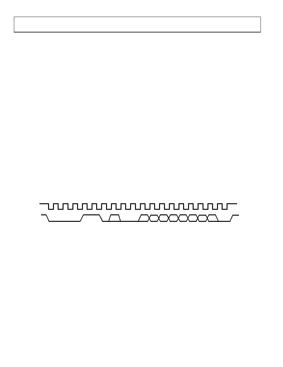
GENERAL I2C TIMING
Figure 25 shows the timing diagram for general read and write
operations using the I2C-compliant interface.
The master initiates data transfer by establishing a start condition,
defined as a high-to-low transition on the serial data line (SDA)
while the serial clock line (SCL) remains high. This indicates
that a data stream follows. The slave responds to the start condition
and shifts in the next 8 bits, consisting of a 7-bit slave address
(MSB first) and an R/W bit, which determines the direction of
the data transfer, that is, whether data is written to or read from
the slave device (0 = write, 1 = read).
The slave responds by pulling the data line low during the low
period before the ninth clock pulse, known as the acknowledge
bit, and holding it low during the high period of this clock
pulse. All other devices on the bus remain idle while the selected
device waits for data to be read from or written to it. If the R/W
bit is 0, the master writes to the slave device. If the R/W bit is 1,
the master reads from the slave device.
Data is sent over the serial bus in sequences of nine clock
pulses, 8 bits of data followed by an acknowledge bit, which can
be from the master or slave device. Data transitions on the data
line must occur during the low period of the clock signal and
remain stable during the high period because a low-to-high
transition when the clock is high can be interpreted as a stop
signal. If the operation is a write operation, the first data byte
after the slave address is a command byte. This tells the slave
device what to expect next. It may be an instruction telling the
slave device to expect a block write, or it may be a register address
that tells the slave where subsequent data is to be written. Because
data can flow in only one direction as defined by the R/W bit, it
is not possible to send a command to a slave device during a
read operation. Before performing a read operation, it is sometimes
necessary to perform a write operation to tell the slave what sort
of read operation to expect and/or the address from which data
is to be read.
When all data bytes are read or written, stop conditions are
established. In write mode, the master pulls the data line high
during the 10th clock pulse to assert a stop condition. In read
mode, the master device releases the SDA line during the low
period before the ninth clock pulse, but the slave device does
not pull it low. This is known as a no acknowledge. The master
then takes the data line low during the low period before the
10th clock pulse, and then high during the 10th clock pulse to
assert a stop condition.
0
1
0
1
R/W
D7
D6
D5
D4
D3
D2
D1
D0
START CONDITION
BY MASTER
ACKNOWLEDGED BY
AD5934
SLAVE ADDRESS BYTE
ACKNOWLEDGED BY
MASTER/SLAVE
SCL
SDA
REGISTER ADDRESS
05325-
048
Figure 25. Timing Diagram
相关PDF资料 |
PDF描述 |
|---|---|
| AD598JR | IC LVDT SGNL COND OSC/REF 20SOIC |
| AD660BR | IC DAC 16BIT MONO W/VREF 24-SOIC |
| AD6620ASZ | IC DGTL RCVR DUAL 67MSPS 80-PQFP |
| AD6623ASZ | IC TSP 4CHAN 104MSPS 128MQFP |
| AD6641BCPZRL7-500 | IC IF RCVR 11BIT 200MSPS 56LFCSP |
相关代理商/技术参数 |
参数描述 |
|---|---|
| AD5934YRSZ-REEL7 | 功能描述:IC CONV 12BIT 250KSPS 16SSOP RoHS:是 类别:集成电路 (IC) >> 接口 - 直接数字合成 (DDS) 系列:- 产品变化通告:Product Discontinuance 27/Oct/2011 标准包装:2,500 系列:- 分辨率(位):10 b 主 fclk:25MHz 调节字宽(位):32 b 电源电压:2.97 V ~ 5.5 V 工作温度:-40°C ~ 85°C 安装类型:表面贴装 封装/外壳:16-TSSOP(0.173",4.40mm 宽) 供应商设备封装:16-TSSOP 包装:带卷 (TR) |
| AD594 | 制造商:AD 制造商全称:Analog Devices 功能描述:Monolithic Thermocouple Amplifiers with Cold Junction Compensation |
| AD594A | 制造商:AD 制造商全称:Analog Devices 功能描述:Monolithic Thermocouple Amplifiers with Cold Junction Compensation |
| AD594AD | 制造商:Analog Devices 功能描述:Temp Sensor Analog 14-Pin TO-116 制造商:Rochester Electronics LLC 功能描述:THERMOCOUPLER AMPLIFIER - Bulk 制造商:Analog Devices 功能描述:Special Function IC Package/Case:TO-116 |
| AD594AD/+ | 制造商:Rochester Electronics LLC 功能描述:- Bulk |
发布紧急采购,3分钟左右您将得到回复。